Sumitomo Bakelite Co., Ltd. has announced the expansion of production capacity for encapsulants for advanced semiconductors at its Suzhou plant in China and its Singapore base. The move comes as the company strengthens its global supply system to meet the rapidly growing demand for advanced packaging associated with the spread of generative AI and communication satellites.
- Key Points of the Production Expansion Plans in Suzhou, China, and Singapore
- Performance Evolution of Encapsulants Required for Advanced Semiconductor Packaging
- Restructuring Global Supply Chains Through Acquisitions and Facility Expansion
- Structural Changes Brought by the Generative AI Boom and Market Expansion
- The time lag between upfront investment and quality certification unique to materials manufacturers
- Future Outlook and Key Focus Areas for Next-Generation Packaging
Key Points of the Production Expansion Plans in Suzhou, China, and Singapore
On October 9, 2026, Sumitomo Bakelite Co., Ltd. announced that it will significantly increase its production capacity for encapsulants for advanced semiconductor packages in Suzhou, China, and Singapore. Specifically, new production lines for the “Sumicon EME” encapsulant for molded underfill (MUF) and the “Sumicon EME Version GR” granular encapsulant for compression molding will be introduced at both locations. At Sumitomo Bakelite (Suzhou) Co., Ltd. in China, a new building will be added on the premises of the new plant completed in 2024, with production aiming to start in fiscal 2030. Infrastructure reinforcement will proceed at this site, which has a total area of approximately 60,000 square meters. Meanwhile, at the Singapore base, which has a site area of approximately 22,500 square meters, new lines will be added within the existing factory, with production scheduled to start by the end of fiscal 2028. Please refer to the figure below.
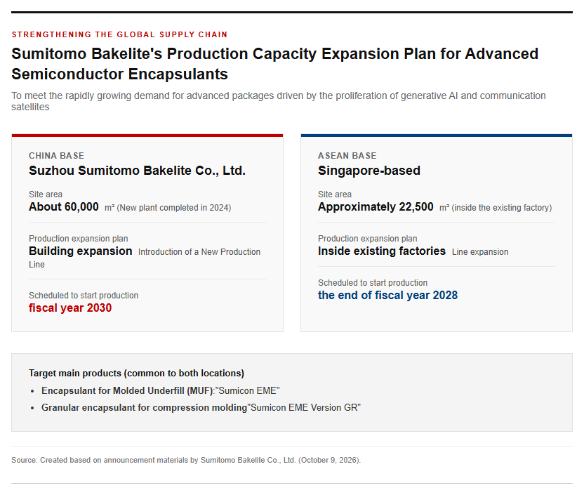
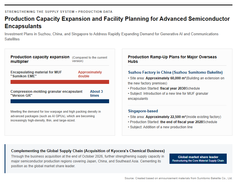
With this capital investment, the company’s production capacity for MUF encapsulants is expected to approximately double from its current level, while production capacity for granular encapsulants will expand about threefold. Furthermore, with the scheduled acquisition of the chemical business from Kyocera Corporation at the end of October 2026, the structure is set to further strengthen supply capabilities across major semiconductor production regions encompassing Japan, China, and Southeast Asia.
Performance Evolution of Encapsulants Required for Advanced Semiconductor Packaging
Semiconductor encapsulants are essential materials that protect semiconductor chips from heat, moisture, and external physical shocks. In advanced semiconductors used for applications such as generative AI GPUs and communication satellites, packaging is rapidly advancing in terms of higher density, thinner profiles, larger sizes, and multi-tier stacking. Along with this, encapsulants are increasingly required to provide advanced functions that go beyond mere protection, such as controlling the mechanical stress and warpage of the entire structure. The MUF encapsulants offered by the company feature excellent fillability into minute gaps and low warpage, simultaneously achieving high manufacturing efficiency and joint reliability by performing the filling of solder joints and the encapsulation of the entire package in a single step. Furthermore, granular encapsulants for compression molding exhibit uniform moldability and low warpage even on large panels, thanks to technology that optimally controls filler size, resin viscosity, and granule particle size. Such evolution in material technology is directly linked to improving the yield and productivity of advanced semiconductor packages, shifting their role from conventional, purely protective components to core materials that make the package structure possible. Sumitomo Bakelite is rapidly responding to these sophisticated market demands by leveraging its proprietary compounding design technology.
Restructuring Global Supply Chains Through Acquisitions and Facility Expansion
Sumitomo Bakelite has established a leading global market share in semiconductor encapsulants. In addition to these large-scale investments in two locations, the acquisition of Kyocera’s chemical business, scheduled for completion at the end of October 2026, will integrate the company’s strengths in high-heat-dissipation technology and the memory sector, as well as its production capacity for MUF and granular encapsulants. This will further enhance its competitive advantage in the AI semiconductor sector, where thermal management is the utmost priority. Please refer to the figure below.
Due to geopolitical factors, the U.S.-China conflict, and the strengthening of economic security policies, the semiconductor supply chain is progressing from its conventional heavy concentration in East Asia toward decentralization and diversification into regions such as Southeast Asia. The company is promoting the duplication of production systems and multi-fab operations across its major bases in Japan, China, and Southeast Asia, adopting a strategy to mitigate regional procurement and geopolitical risks. From the perspective of business continuity planning (BCP), it is also advancing the securing of appropriate inventory and the establishment of alternative production systems, and by building a stable supply network closely aligned with its major production sites, it aims to maintain and expand its long-term business relationships with client companies and its market share.
Structural Changes in the Semiconductor Materials Market and Future Investment Outlook
Structural Changes Brought by the Generative AI Boom and Market Expansion
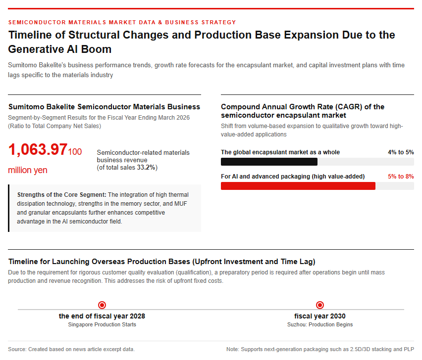
The rapid adoption of GPUs and high-bandwidth memory (HBM) for AI servers, as well as edge AI for smartphones and PCs, is strongly driving the growth of the entire semiconductor materials market. Looking at Sumitomo Bakelite’s segment sales for the fiscal year ending March 2026, the semiconductor-related materials business reached 106.397 billion yen, making it a core segment that accounts to 33.2% of total sales. While the compound annual growth rate (CAGR) of the global semiconductor encapsulant market as a whole is expected to show steady growth of around 4% to 5%, high-value-added applications—such as ultra-small, low-warp grades for AI and advanced packaging—are expected to achieve high growth rates equivalent to 5% to 8% annually. In other words, the encapsulant market is undergoing a structural shift from mere volume-based expansion to qualitative growth centered on improvements in product unit prices and grades driven by higher functionality. The company offers a diverse product lineup, including thermal management materials for power semiconductors, “LaZ” substrate materials, and liquid encapsulants, establishing a system to directly capture the expansion of AI demand into business performance growth.
The time lag between upfront investment and quality certification unique to materials manufacturers
A notable point in this capital investment is the existence of a time lag characteristic of the materials industry, which requires a considerable period from the investment decision to actual profit contribution. Production in Singapore is scheduled to begin at the end of fiscal 2028, and in Suzhou in fiscal 2030, several years from now. In the semiconductor materials sector, even after new plants and new lines begin operations, slight differences in the physical properties of products affect customer yields and reliability, requiring rigorous quality evaluation and qualification processes by the customer. Consequently, in addition to the construction period, additional preparatory time is required before actual mass shipments and sales recording can take place. Meanwhile, fixed costs such as depreciation and labor expenses are incurred ahead of time with the completion of the plant, which can temporarily weigh on profits in the initial startup phase. Because starting investment after a sudden surge in demand risks missing business opportunities, the importance of management decisions to proactively secure production capacity while improving the accuracy of future demand forecasting is growing.
Future Outlook and Key Focus Areas for Next-Generation Packaging
Key points to watch moving forward include the further functional enhancement of encapsulation materials driven by the advancement of next-generation packaging technologies such as 2.5D and 3D stacking, and panel-level packaging (PLP). By pushing formulation design technology to its absolute limits, Sumitomo Bakelite is striving to achieve a reduced coefficient of thermal expansion during high-density mounting, as well as a balance between high rigidity and toughness. Please refer to the figure below.
Furthermore, the company’s technical positioning is expected to be further strengthened as sample shipments of liquid encapsulants for GPUs progress and high-heat-dissipation technologies are integrated through the acquisition of Kyocera’s chemical business. While passing on fluctuations in raw material prices through the application of pricing formulas, the company will be required to continue multi-sourcing as a countermeasure against geopolitical risks and supply chain fragmentation. Whether the new lines, which are scheduled to begin operations sequentially from the end of fiscal 2028 through fiscal 2030, obtain certification as planned and translate market expansion into earnings will be the primary focal point for enhancing corporate value over the medium to long term.
Reference Page
- 【Regarding the Expansion of Production Capacity for Advanced Semiconductor Encapsulation Materials in Suzhou, China and Singapore | Sumitomo Bakelite Co., Ltd.】[suspicious link removed]
【#SumitomoBakelite #SemiconductorEncapsulants #AISemiconductors #MoldUnderfill #SemiconductorMaterials #AdvancedPackaging #SupplyChain】

コメント