Kumamoto University, Yamagata University, and Germany’s Fraunhofer-Gesellschaft have signed a comprehensive partnership agreement to conduct joint research on semiconductor packaging and assembly technologies. This initiative is driven by the growing importance of back-end packaging amidst physical miniaturization limits, alongside efforts to strengthen the global expansion of regional industries.
- Comprehensive Partnership Agreement Signed by Four Japanese and German Institutions in September 2026
- Framework for Supporting Overseas Partnerships via JETRO Kumamoto and Local Consortia
- Overview of International Joint Research in Semiconductor Back-End Processing
- Physical Limits of Miniaturization and Challenges to Moore’s Law
- Mechanics of Chiplet Integration and Heterogeneous Integration
- High-Density Integration and Low Power Consumption via Interposers and 3D Stacking
- Semiconductor Packaging Workshop Hosted at Kumamoto University
- Strengthening Regional Industrial Competitiveness and Future Key Focuses
Comprehensive Partnership Agreement Signed by Four Japanese and German Institutions in September 2026
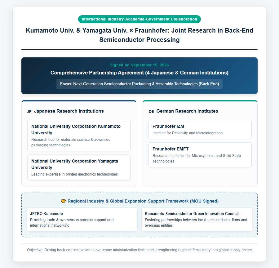
On September 10, 2026, a signing ceremony for a comprehensive partnership agreement was held among four institutions: Kumamoto University, Yamagata University, and two institutes under Europe’s largest applied research organization, Fraunhofer-Gesellschaft—namely Fraunhofer IZM (Institute for Reliability and Microintegration) and Fraunhofer EMFT (Research Institution for Microsystems and Solid State Technologies). The agreement aims to promote international joint research and technological development in back-end processes, specifically packaging and assembly, which are increasingly crucial in next-generation semiconductor manufacturing. In conjunction with the signing ceremony, related events such as a Japan-Germany joint workshop were organized, launching a robust collaborative framework uniting industry, academia, and government across both nations. By combining Japan’s regional hubs—led by Kumamoto Prefecture, a rapidly growing semiconductor cluster—with Europe’s leading research institutions, this initiative is expected to yield innovative research breakthroughs in advanced back-end technologies.
Framework for Supporting Overseas Partnerships via JETRO Kumamoto and Local Consortia
Parallel to the academic and technological collaboration between universities and research institutes, a key memorandum of understanding (MOU) was concluded between the Japan External Trade Organization (JETRO Kumamoto), which promotes overseas expansion and trade support for domestic companies, and the Kumamoto Semiconductor Green Innovation Council, comprising regional semiconductor-related businesses. Under this MOU, both entities will leverage their international networks and regional industrial bases to significantly deepen ties between local businesses in Kumamoto’s semiconductor sector and overseas research organizations and enterprises. Moving beyond purely academic research, this multi-faceted support system aims to build an environment where local industries gain direct access to global supply chains and technological ecosystems, driving foreign corporate investment, joint project creation, and sustainable regional economic growth.
Overview of International Joint Research in Semiconductor Back-End Processing
The core focus of this joint research lies in “back-end processing,” which encompasses the manufacturing steps after circuit pattern formation on silicon wafers: dicing, mounting onto substrates, packaging, and final testing. In contemporary semiconductor engineering, relying solely on circuit pattern miniaturization in front-end processing to boost performance has become physically and economically challenging. Consequently, advanced back-end packaging technologies have emerged as the decisive factor determining overall semiconductor performance and power efficiency. This joint research project integrates the advanced material science and printed electronics expertise of Kumamoto University and Yamagata University with Fraunhofer’s long-established capabilities in high-density packaging and reliability evaluation. Together, the partner institutions aim to establish innovative assembly technologies to power next-generation communications and AI processing.
The Critical Role of Back-End Packaging and Chiplets in Overcoming Fabrication Barriers
Physical Limits of Miniaturization and Challenges to Moore’s Law
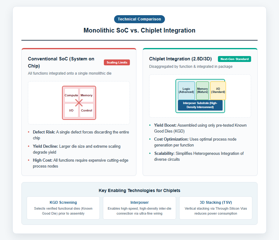
For decades, semiconductor advancement was guided by Moore’s Law—the observation by Gordon Moore in 1965 that the number of transistors on a microchip doubles roughly every two years, driving performance gains and cost reductions. However, as circuit feature sizes reach the extreme scale of just a few nanometers, the industry faces severe physical hurdles, including quantum interference, leakage currents, and declining yields due to manufacturing complexity. Furthermore, constructing and operating cutting-edge front-end fabrication facilities requires astronomical capital investments, bringing traditional performance scaling reliant purely on miniaturization to its financial limit. Conventional System-on-Chip (SoC) architectures, where a single defect invalidates an entire monolithic chip, inevitably suffer from degraded manufacturing efficiency, necessitating a fundamental redesign of semiconductor architecture.
Mechanics of Chiplet Integration and Heterogeneous Integration
To overcome miniaturization limits, “chiplet” technology has rapidly gained global adoption. Instead of fabricating a massive, complex system on a single monolithic SoC, chiplet architecture disaggregates functional blocks—such as compute cores, memory controllers, and I/O—into smaller individual dies, which are then integrated into a single unified package. By utilizing only pre-tested, verified functional dies (Known Good Die, or KGD), overall manufacturing yield improves dramatically. Furthermore, applying “heterogeneous integration”—combining dies made with different process nodes or materials within the same package—allows designers to optimize cost and performance. Advanced, expensive process nodes can be reserved for compute-intensive logic, while memory and analog circuits utilize mature, cost-effective legacy nodes.
High-Density Integration and Low Power Consumption via Interposers and 3D Stacking
Connecting multiple chiplets at high speeds and densities requires a critical intermediary layer known as an “interposer.” Acting as a high-density wiring substrate made of silicon, organic materials (RDL), or glass, the interposer features ultra-fine interconnects with micro-pitch electrodes that drastically reduce signal latency and power loss. Furthermore, technology is evolving from 2.5D integration—where dies are arranged side-by-side on an interposer—to three-dimensional (3D) integration, which stacks dies vertically using Through-Silicon Vias (TSVs). By vertically aligning memory and logic circuits, physical interconnect distances are minimized to the extreme, achieving massive data bandwidths and groundbreaking energy efficiency essential for intensive AI computations.
Japan-Germany Joint Workshop and Future Industrial and Societal Impact
Semiconductor Packaging Workshop Hosted at Kumamoto University
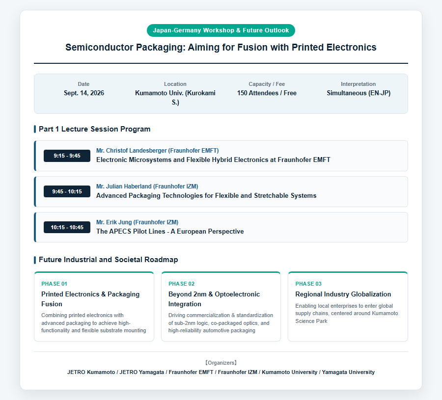
Following the partnership agreement, the Japan-Germany Joint Workshop titled “Semiconductor Packaging: Aiming for Fusion with Printed Electronics” was held on September 14, 2026, at the Kurokami South Campus of Kumamoto University’s Faculty of Engineering. Co-hosted by JETRO Kumamoto, JETRO Yamagata, Fraunhofer EMFT, Fraunhofer IZM, Kumamoto University, and Yamagata University, the event drew a full capacity of 150 participants. Visiting researchers from Fraunhofer delivered cutting-edge lectures on flexible hybrid electronics and advanced packaging technologies for flexible and stretchable systems. Simultaneous English-Japanese interpretation was provided during the first session, fostering active exchanges between Japanese and German researchers and local industry representatives on fusing advanced packaging with printed electronics.
Strengthening Regional Industrial Competitiveness and Future Key Focuses
The Kyushu region, centered around Kumamoto Prefecture, has become a primary engine driving Japan’s semiconductor resurgence, bolstered by the entry of major foundries and the development of innovation hubs such as Kumamoto Science Park. The joint research initiative between Kumamoto University, Yamagata University, and Fraunhofer, alongside support from JETRO and regional consortia, provides a solid foundation for local enterprises to adapt swiftly to advanced back-end technological shifts and global standardization. Looking ahead, key points of interest will focus on how Japanese academic bases and European research prowess collaborate to commercialize beyond-2nm ultra-advanced logic, co-packaged optics (CPO), and high-reliability automotive packaging, ultimately contributing to resilient global supply chains and a low-power digital society.
References
- [2026 Press Releases | Kumamoto University] https://www.kumamoto-u.ac.jp/daigakujouhou/kouhou/pressrelease/2026
- [Japan-Germany Joint Workshop “Semiconductor Packaging” ~Aiming for Fusion with Printed Electronics~] https://www.fraunhofer.jp/ja/events/event2026/joint26.html
- [What is “Chiplet”, the Key to Next-Generation Semiconductor Manufacturing? | Rapidus Corporation] https://www.rapidus.inc/tech/te0002/
【#Semiconductors #KumamotoUniversity #YamagataUniversity #Fraunhofer #Chiplets #BackEndProcess #InternationalJointResearch #TechnologicalInnovation】


コメント