IC-Link, a business unit of the Belgian research hub imec, and TSMC have announced an expanded collaboration in cloud-enabled advanced semiconductor design. The partnership comes as extreme miniaturization dramatically increases design complexity, driving the need to ease development infrastructure burdens for emerging fabless firms and research institutions.
- Joining the OIP Cloud Alliance and Enabling Mixed-Partner EDA Flows
- Escalating Design Complexity and Challenges for Next-Gen Chipmakers
- Flexible Tool Integration and Secure Access to TSMC’s Advanced PDKs
- Deepening a Multidecade Partnership to Empower Startup Ecosystems
- Strengthening the European Semiconductor Ecosystem and Global Innovation
- Navigating the Agentic AI Design Era: Opportunities and Operational Challenges
Joining the OIP Cloud Alliance and Enabling Mixed-Partner EDA Flows
On September 23, 2026, IC-Link—the ASIC management unit of Belgian research institution imec—and Taiwan Semiconductor Manufacturing Company (TSMC) announced an expansion of their long-standing collaboration during an event in Santa Clara, California. Under this agreement, IC-Link has officially joined TSMC’s Open Innovation Platform (OIP) Cloud Alliance. IC-Link will deliver the industry’s first managed cloud service capable of supporting mixed-partner Electronic Design Automation (EDA) flows, allowing design teams to seamlessly integrate tools from multiple vendors within a unified cloud environment. This setup enables developers to securely access TSMC’s advanced Process Design Kits (PDKs) under strict governance. Historically, establishing cloud-based design environments required major corporations to build proprietary infrastructures or rely heavily on single-vendor stacks. By contrast, this managed service offers small and medium-sized design teams a flexible alternative, significantly accelerating their path to advanced semiconductor manufacturing nodes.
Escalating Design Complexity and Challenges for Next-Gen Chipmakers
As the semiconductor industry transitions into the angstrom era—marked by 2-nanometer and 1.4-nanometer (A14) nodes—the physical and structural complexity of circuit design and 3D packaging has surged exponentially. Consequently, chip design teams worldwide face formidable hurdles, including securing vast computing capacity, maintaining robust cybersecurity, and bearing exorbitant infrastructure overhead. In high-growth sectors such as Artificial Intelligence (AI), telecommunications, automotive, and industrial automation, accelerating time-to-market is critical to commercial success. However, engineering teams frequently find their resources drained by the arduous process of configuring secure environments capable of running diverse EDA tools while complying with intricate PDK rules. This administrative overhead diverts focus from core innovation. The industry has thus urgently demanded a flexible, managed infrastructure that streamlines the entire development lifecycle, from initial architectural concept to commercial tape-out.
How IC-Link’s Managed Cloud Infrastructure Works
Flexible Tool Integration and Secure Access to TSMC’s Advanced PDKs
The primary strength of IC-Link’s managed cloud environment lies in its architecture, which seamlessly balances operational flexibility with enterprise-grade security. Customer design teams can bring their existing EDA toolchains and vendor licenses under a Bring Your Own License (BYOL) model directly into the cloud platform. IC-Link manages the heavy lifting, taking full responsibility for secure hosting, strict access control over TSMC’s cutting-edge PDKs, and dynamic compute resource scaling based on real-time design loads. The following diagram illustrates the concept of this collaborative cloud-enabled design framework:
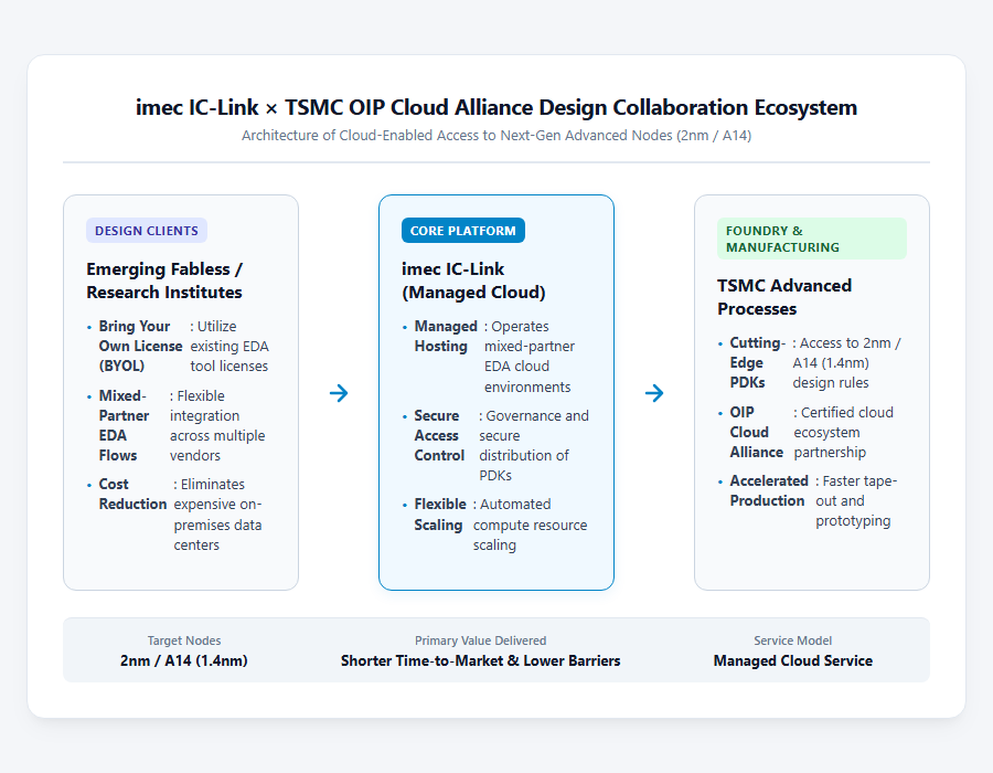
By removing the burden of maintaining expensive on-premises data centers and complex verification hardware, this managed infrastructure allows emerging fabless startups, universities, and research institutes to smoothly participate in advanced chip development using TSMC’s newest process technologies.
Deepening a Multidecade Partnership to Empower Startup Ecosystems
This initiative builds upon a solid foundation of collaboration between imec and TSMC spanning nearly two decades. IC-Link previously joined TSMC’s Design Center Alliance (DCA) in 2007, its Value Chain Alliance (VCA) in 2009, and more recently, the 3DFabric Alliance focused on advanced packaging technologies. While previous alliance memberships focused primarily on specialized technical enablement and packaging solutions, joining the OIP Cloud Alliance extends their synergistic relationship directly into cloud infrastructure. Historically, leading-edge node development was the exclusive domain of well-funded tech giants and hyperscalers. Delivering advanced design infrastructure as a managed service significantly lowers the barrier to entry for startups. For TSMC, this strategic expansion creates a valuable pipeline to engage and nurture the next generation of high-growth semiconductor innovators early in their development lifecycle.
Broader Industry Impact and Future Outlook
Strengthening the European Semiconductor Ecosystem and Global Innovation
The expansion of this partnership extends far beyond a single corporate service offering, delivering substantial benefits across both regional and global semiconductor ecosystems. Across Europe, major strategic initiatives such as the EU Chips Act and the NanoIC Pilot Line are actively building up advanced manufacturing and research capacities. IC-Link’s enhanced managed cloud capabilities serve as a vital bridge, enabling European research centers and startups to rapidly transform cutting-edge chip prototypes into volume production. The following diagram demonstrates the expanding innovation architecture connecting research institutions directly to manufacturing foundries:
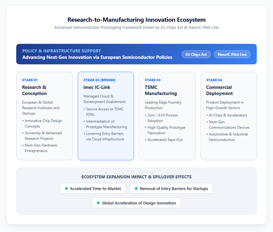
Furthermore, by democratizing access to state-of-the-art process technologies for innovative engineers globally, this framework is poised to accelerate hardware breakthroughs in AI accelerators, next-generation wireless communications, and automotive electronics.
Navigating the Agentic AI Design Era: Opportunities and Operational Challenges
A critical trend shaping the future of semiconductor development is the integration of autonomous, agentic AI into design workflows. At the 2026 TSMC OIP Ecosystem Forum, leading EDA vendors including Cadence, Synopsys, and Siemens unveiled production-ready AI agent capabilities tailored for TSMC’s sub-2nm and A14 process nodes. While these automated AI agents dramatically compress development cycles by autonomously performing design repairs and verification, they also demand immense cloud computing power over extended runtime periods. A pivotal operational challenge for IC-Link’s managed cloud will be sustaining a scalable capacity model capable of accommodating these heavy AI workloads. Moving forward, the industry will closely monitor IC-Link’s customer adoption rate outside Europe, as well as the accumulation of verified tape-out milestones on leading-edge process nodes.
References
- [IC-Link by imec expands collaboration with TSMC to accelerate customer access to advanced-node chip design infrastructure and support] https://www.imec-int.com/en/press/ic-link-imec-expands-collaboration-tsmc-accelerate-customer-access-advanced-node-chip-design

コメント