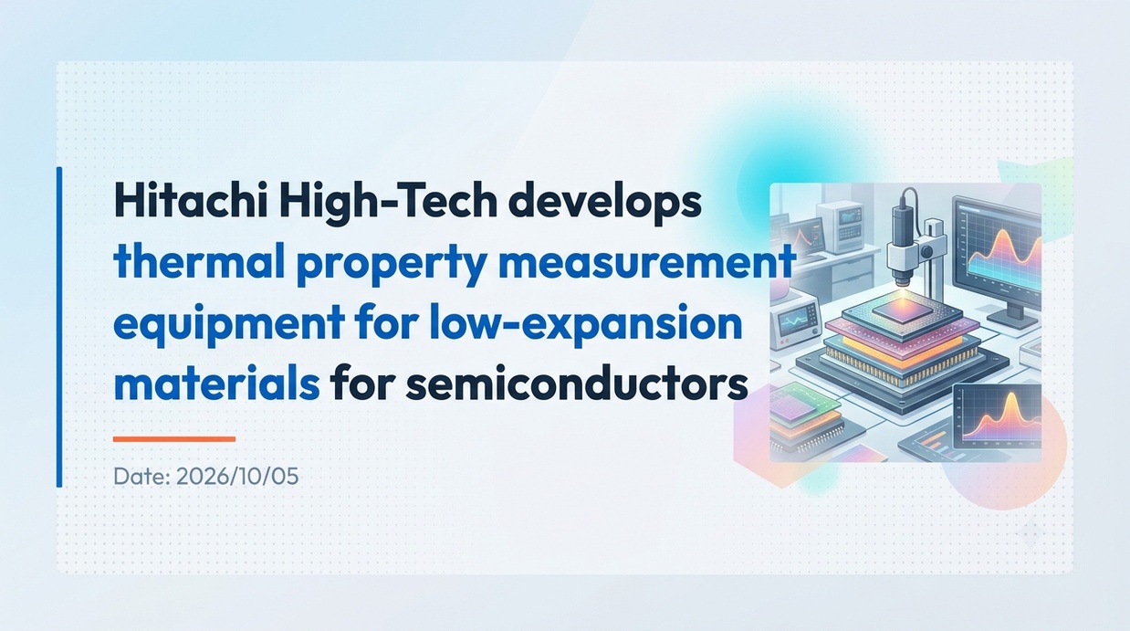
Hitachi High-Tech has developed the “NEXTA DMA200” dynamic mechanical analyzer, which evaluates the thermal characteristics of low-expansion materials for advanced semiconductor packages with high precision. This comes against the backdrop of increasingly severe issues with thermal warpage and stress relaxation associated with the high-density stacking of AI server semiconductors and the integration of heterogeneous materials.
- Key Points of the Event and Background on Semiconductor Advancement
- Mechanism of Thermal Warpage and Stress Generation Due to Dissimilar Material Lamination
- High load output of up to 20N and high-precision control via a dedicated DAC
- Environmental and Safety Considerations via Liquid Nitrogen-Free Electric Gas Chiller Cooling
- Improving Quality and Shortening Development Time for Package Substrates and Encapsulation Materials
- Future Developments and Future Outlook for Semiconductor Packaging Technology
Key Points of the Event and Background on Semiconductor Advancement
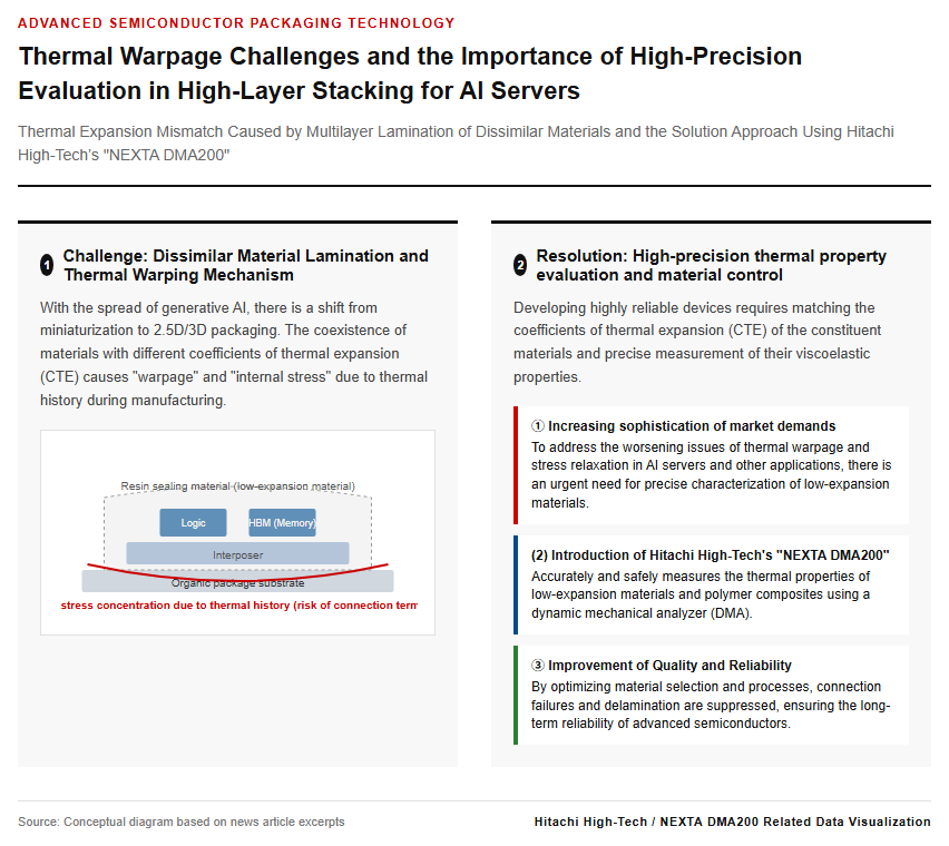
In recent years, with the rapid adoption of generative AI and high-performance computing, the focus of performance improvement in semiconductor devices has shifted from conventional circuit miniaturization to advanced packaging technologies such as 2.5D and 3D integration. In such high-density packages, multi-layered structures in which various dissimilar materials with different coefficients of thermal expansion—such as silicon chips, interposers, organic package substrates, and resin encapsulants—are laminated have become mainstream. Due to the thermal history of heating and cooling during the manufacturing process, differences in thermal shrinkage occur among the components, and the generation of warpage and internal stress throughout the package has emerged as a serious quality issue. Because warpage leads to the detachment of fine connection terminals and poor contact, which significantly impairs the long-term reliability of products, precise control over the matching of coefficients of thermal expansion and the viscoelastic properties of the constituent materials is essential. To meet these market demands, Hitachi High-Tech has developed the NEXTA DMA200 dynamic mechanical analyzer, which can measure the thermal properties of low-expansion materials and polymer composites with high precision and safety, and has begun providing it to research and development sites for advanced semiconductor materials.
Mechanism of Thermal Warpage and Stress Generation Due to Dissimilar Material Lamination
Inside advanced semiconductor packages, severe thermal loads are constantly applied due to heat generation during operation and the curing process of sealing resins. While the coefficient of thermal expansion (CTE) of silicon is on the order of a few ppm per degree, the CTEs of substrate and resin materials reach several tens of ppm per degree, causing the gap in expansion and contraction associated with temperature changes to accumulate as internal stress. Especially in HBM, which is advancing toward high integration exceeding 16 layers, and large-scale panel-level packages, even a slight difference in shrinkage causes significant structural deformation. To suppress this warping phenomenon, it is necessary to accurately capture the dynamic viscoelastic behavior of low thermal expansion substrate materials, solder resists, and liquid encapsulants developed by material manufacturers. Specifically, precisely grasping the decrease in storage modulus accompanying temperature changes and the peaks of loss modulus and loss tangent near the glass transition temperature determines the success or failure of the design. Building an evaluation system capable of measuring microscopic deformations and a wide range of elastic moduli—which was difficult with conventional methods—holds the greatest key to improving manufacturing yields for next-generation devices.
Innovative Technical Features of the NEXTA DMA200 Dynamic Mechanical Analyzer
High load output of up to 20N and high-precision control via a dedicated DAC
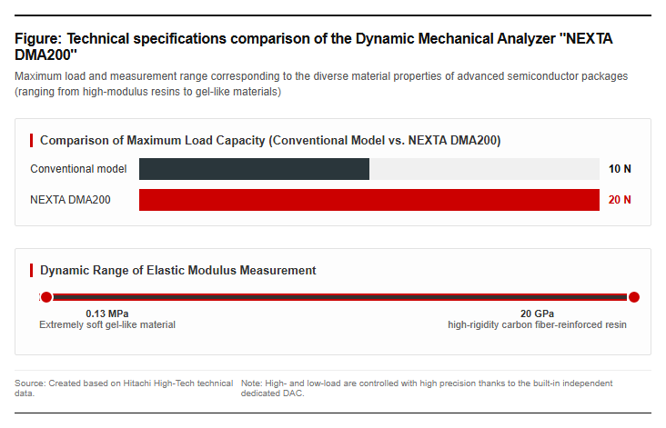
Developed by Hitachi High-Tech, the NEXTA DMA200 dynamic mechanical analyzer adopts a new structure that significantly overcomes the limitations in modulus measurement inherent in conventional measuring devices. To sufficiently deform and measure highly elastic materials such as high-rigidity carbon fiber reinforced plastics, powerful magnets are positioned in the force generation unit and the coil winding structure has been optimized, achieving a maximum load output of 20N—double the 10N maximum load of conventional models. On the other hand, when measuring thinned semiconductor encapsulant films or soft, low-elasticity materials, high load resolution capable of precisely controlling minute loads is required. In general devices, there has been a challenge where the control resolution decreases as the maximum load increases; however, this device features a newly developed circuit configuration equipped with separate, dedicated D/A converters independently for high-load output and low-load output. This has successfully secured an exceptional dynamic range that enables stable measurement with a single device, ranging from highly elastic reinforced plastics reaching 20 GPa to extremely soft gel-like materials of about 0.13 MPa.
Environmental and Safety Considerations via Liquid Nitrogen-Free Electric Gas Chiller Cooling
When evaluating the viscoelastic properties of semiconductor and polymer materials at low temperatures, a cooling unit using liquid nitrogen has conventionally been essential to reach cryogenic regions of minus 100 degrees Celsius or lower. However, the use of liquid nitrogen has involved operational challenges, such as ensuring operator safety, managing the risk of asphyxiation, and high running costs associated with the constant replenishment of the refrigerant. The NEXTA DMA200 supports a proprietary cooling method using an electric gas chiller, enabling rapid cooling down to minus 100 degrees using only a power connection, without using any liquid nitrogen. By employing a mechanism in which dry air is cooled down to minus 120 degrees by an internal compressor and introduced directly into the sample section, it achieves high cooling performance, reaching minus 100 degrees in just about 10.2 minutes from the start of cooling. While improving work environment safety and reducing environmental impact, this makes it possible to dramatically improve experimental efficiency through shortened test cycles.
Practical Value and Industrial Impact in Advanced Semiconductor Material Development
Improving Quality and Shortening Development Time for Package Substrates and Encapsulation Materials
In the manufacturing process of advanced semiconductor packaging, a wide variety of functional materials are used, including photosensitive solder resists, non-conductive films, and capillary underfills. Because these materials directly dictate package warpage due to shrinkage during thermosetting and distortion when cooling, material selection based on high-precision thermal property data is indispensable. By introducing the NEXTA DMA200, R&D engineers are now able to track material deformation and changes in elastic modulus associated with temperature ramps in real-time and with high resolution. Particularly in the development of cutting-edge package substrate materials and film-like solder resists that achieve both high thermal conductivity and low expansion, an environment has been established where the viscoelastic behavior of prototype materials can be rapidly fed back. This significantly accelerates the proof-of-concept and specification optimization processes for packaging materials, which previously took several months, greatly contributing to shortening the time-to-market for next-generation AI semiconductor products.
Future Developments and Future Outlook for Semiconductor Packaging Technology
Driven by the expanding demand for generative AI and high-performance semiconductors for automotive applications, the market size for semiconductor manufacturing equipment and related materials is expected to continue expanding rapidly on a global scale. According to demand forecasts by the Semiconductor Equipment Association of Japan, sales of Japanese semiconductor manufacturing equipment for fiscal 2026 are estimated to reach 6.5502 trillion yen, a 26 percent increase over the previous fiscal year, and high-level growth is projected to continue thereafter. As the importance of back-end packaging technology continues to grow, precise evaluation technology for material properties serves as the cornerstone for improving device yields and ensuring reliability. Hitachi High-Tech plans to support the development of the global semiconductor supply chain through the deployment of HMAX, an integrated solution leveraging core technologies cultivated in the measurement and analysis systems field, AI image processing, and physical AI. The advancement of thermal analysis technology will continue to play a crucial role as a foundation supporting the societal implementation of anticipated innovative technologies such as 3D stacking and optoelectronic fusion.
Reference Page
- [Features and Measurement Examples of the Dynamic Mechanical Analyzer NEXTA DMA200 : SI NEWS : Hitachi High-Tech] https://www.hitachi-hightech.com/jp/ja/sinews/technology/6220326/
- 【Materials Contributing to Warpage Suppression and Stress Relaxation in Advanced Semiconductor Packages: Resonac】https://www.resonac.com/jp/solution/column/007.html
- [Precision Measurement of Thermal Expansion Properties: AIST Magazine] https://www.aist.go.jp/aist_j/magazine/20250515.html
【#HitachiHighTech #SemiconductorPackaging #ThermalAnalysis #LowExpansionMaterial #DMA200 #ThermalExpansionCoefficient】


コメント