Ookuma Diamond Device, which recently completed the world’s first diamond semiconductor factory in Okuma Town, Fukushima Prefecture, is exploring partnership agreements with local research institutions and enterprises, including the University of Aizu. This initiative aims to pool diverse regional technologies to establish a robust mass production system ahead of the factory’s full-scale operation scheduled for fiscal year 2028.
- Completion of the World’s First Okuma Factory and the Roadmap to Mass Production
- Collaboration with Local Academia, such as the University of Aizu, and Expectations for Innovation
- Overwhelming Physical Properties Breaking Through the Limits of Existing Materials
- Unique Vertically Integrated Manufacturing Expertise Forged in Decommissioning Projects
- Job Creation and Sustainable Vitality in Fukushima’s Hamadori Region
- Global Expansion and IP Strategy Targeted at Space, Defense, and Next-Generation Communication Markets
Completion of the World’s First Okuma Factory and the Roadmap to Mass Production
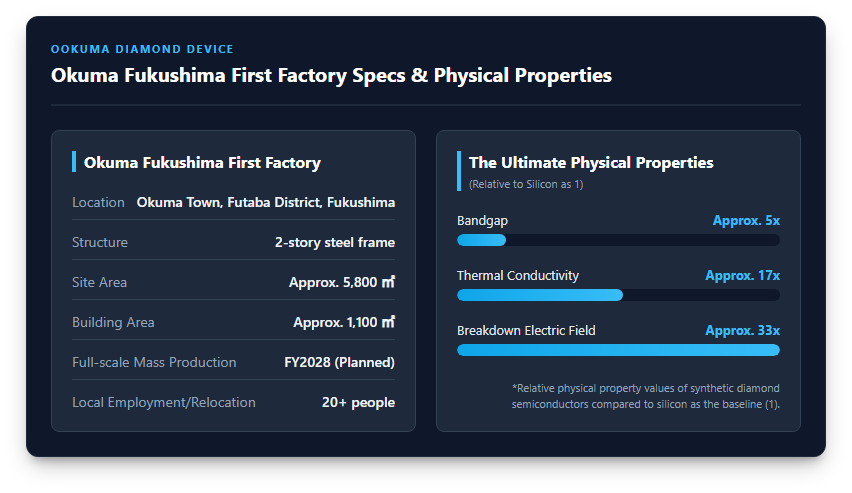
Ookuma Diamond Device Co., Ltd. held the completion ceremony for its Fukushima First Factory in Okuma Town, Futaba District, Fukushima Prefecture, on May 29, 2026. This facility was built as the world’s first mass production factory for diamond semiconductors. In just over four years since its founding in March 2022, the company has established vertically integrated manufacturing expertise, achieving a yield rate of over 90% at the lab scale, and has successfully completed its long-awaited production base. The factory is scheduled for full-scale mass production starting in fiscal year 2028, bringing the commercialization of synthetic diamond semiconductors—often referred to as the “ultimate semiconductor”—closer to reality. Beginning with its contribution to the decommissioning of the Fukushima Daiichi Nuclear Power Station, the company plans to establish a stable and highly precise supply system for devices destined for massive markets requiring stable operation under extreme conditions, such as space exploration and next-generation 6G communications.
The image below shows the exterior of the world’s first diamond semiconductor factory completed in Okuma Town, Fukushima Prefecture.
Collaboration with Local Academia, such as the University of Aizu, and Expectations for Innovation
Ookuma Diamond Device is committed to fostering new local industries rooted in Okuma Town, carrying a mission to lead the reconstruction of Fukushima Prefecture. The key to accelerating its social implementation and development experiments lies in building a broad regional collaborative network within the prefecture. As of March 2026, a company spokesperson noted that in addition to collaborating with measurement-related businesses and institutions, establishing broader connections across the Nakadori and Aizu regions would diversify potential corporate matching and significantly expand the scope of their initiatives. Partnering with regional academia specializing in information science and electronic devices, such as the University of Aizu, alongside measurement and processing companies in Nakadori, will optimize inspection and measurement techniques in the Okuma mass production process. This will improve yield rates, shorten the PDCA cycle required for product development, and establish a solid foundation for launching new industries from Fukushima to the world stage.
Drivers Behind Diamond Semiconductors and Their Technical Advantages
Overwhelming Physical Properties Breaking Through the Limits of Existing Materials
Diamond semiconductors are called “ultimate” due to their physical property values, which overwhelmingly surpass those of existing materials like silicon. Compared to silicon as a baseline (1), synthetic diamond features a bandgap about 5 times wider, breakdown electric field strength approximately 33 times higher, and thermal conductivity roughly 17 times greater. Furthermore, diamond boasts the highest thermal conductivity on Earth at 1,500 to 2,200 W/mK, representing performance that is orders of magnitude superior to conventional heat-dissipating metals like copper and aluminum. These extraordinary physical properties allow devices to operate reliably and stably without degradation, even in extreme conditions of high voltage, high temperature, and high frequency. They are attracting immense expectations as a breakthrough solution for applications where conventional semiconductors fail, including heat dissipation issues in data centers driven by the rise of AI, high-power control in electric vehicles (EVs) to minimize power loss, and radiation-resistant environments in space and inside nuclear reactors.
Unique Vertically Integrated Manufacturing Expertise Forged in Decommissioning Projects
The core strength of Ookuma Diamond Device lies not just in using superior materials, but in its proprietary manufacturing technologies forged through more than a decade of involvement in nuclear decommissioning projects. Triggered by the 2011 Great East Japan Earthquake and the subsequent Fukushima Daiichi Nuclear Power Station accident, the urgent need for robust devices capable of withstanding intense radiation became clear, leading to the launch of a joint national research project in 2012. By consolidating research expertise from the Japan Atomic Energy Agency (JAEA), the National Institute of Advanced Institute of Science and Technology (AIST), and Hokkaido University, the company established a vertically integrated manufacturing process covering everything from substrate design to the assembly of final amplifier products. Although diamond is an exceptionally hard material requiring advanced precision surface control techniques for processing, polishing, planarization, and bonding with other materials, Ookuma Diamond Device has overcome these hurdles to establish an exclusive technological and time-based advantage required for high-yield mass production.
Local Economic Impact and Future Global Expansion
Job Creation and Sustainable Vitality in Fukushima’s Hamadori Region
The operation of the Fukushima First Factory is expected to bring substantial economic benefits to Okuma Town in the Futaba District, as it continues its recovery from the nuclear accident. Ahead of full-scale operations, the company plans to create local jobs and attract residents, aiming for more than 20 direct hires and relocations, which will directly contribute to sustainable community revitalization. Furthermore, by securing selection for the Ministry of Economy, Trade and Industry’s (METI) Subsidy for Business Location to Support Self-Reliance and Return, and utilizing various support systems under the Fukushima Innovation Coast Framework, the company is rapidly matching with local businesses and establishing regional supply chains. This represents a true reconstruction that does not merely return the area to its pre-disaster state (turning a minus to zero) but transforms it into a plus by embedding a cutting-edge deep tech industry, offering Fukushima as a model for sustainable regional growth.
Global Expansion and IP Strategy Targeted at Space, Defense, and Next-Generation Communication Markets
With full-scale factory operations targeted for fiscal year 2028, Ookuma Diamond Device has already charted a concrete business roadmap focused on global market capture. Alongside its immediate priority of developing radiation sensors and critical proximity monitoring systems for monitoring nuclear reactor interiors, its expansion into the space and defense sectors is progressing steadily, highlighted by its selection for the Japan Aerospace Exploration Agency’s (JAXA) Space Strategic Fund program. Furthermore, the market for high-power amplifiers used in ultra-high-speed, high-capacity next-generation 6G mobile communication base stations is projected to grow exponentially within the next few years. Anticipating this market formation, Ookuma Diamond Device has pursued a land-grab style intellectual property strategy, securing a portfolio of core patents covering the entire value chain. This positions the company firmly to become a global rule-maker in the upcoming era of diamond semiconductors.
References
- [Ookuma Diamond Device] Groundbreaking Ceremony Held for the Construction of the World’s First Diamond Semiconductor Factory: https://prtimes.jp/main/html/rd/p/000000008.000120349.html
- The World’s First Diamond Semiconductor Factory is Now Complete!: https://ookuma-dd.com/news/635/
- Ookuma Diamond Device Raises Approximately 4 Billion Yen in Pre-A Round to Build Diamond Semiconductor Factory: https://prtimes.jp/main/html/rd/p/000000005.000120349.html
- Ookuma Diamond Device Co., Ltd. – Fukushima Innovation Coast Framework Company Directory: https://www.fipo.or.jp/company-db
【#DiamondSemiconductors #OokumaDiamondDevice #UniversityOfAizu #FukushimaInnovationCoastFramework #IndustryAcademiaCollaboration #RegionalRevitalization #NextGenerationCommunications #ScienceAndTechnology】


コメント