Furuya Metal Co., Ltd., a major industrial precious metals manufacturer, has completed construction of its New Chitose Factory in Chitose, Hokkaido, establishing a system to roughly double its production capacity for temperature sensors used in semiconductor manufacturing equipment. This expansion is driven by the rapid growth of AI data centers—which is boosting demand for cutting-edge semiconductors—and strong calls to bolster a stable domestic supply chain for manufacturing equipment components.
- Overview of the ¥4.5 Billion New Facility and Production Capacity Doubling
- Role in Chitose’s Emerging Semiconductor Cluster and Joint Product Development
- The Ultra-High Temperature “R-SP Process” and High-Quality Manufacturing Environment
- Strengthening BCP and Supply Stability Through Synergies with the Tsukuba Factory
- Spillover Effects from AI Data Center Demand into Advanced Materials
- Operational Timeline and Key Watchpoints
Overview of the ¥4.5 Billion New Facility and Production Capacity Doubling
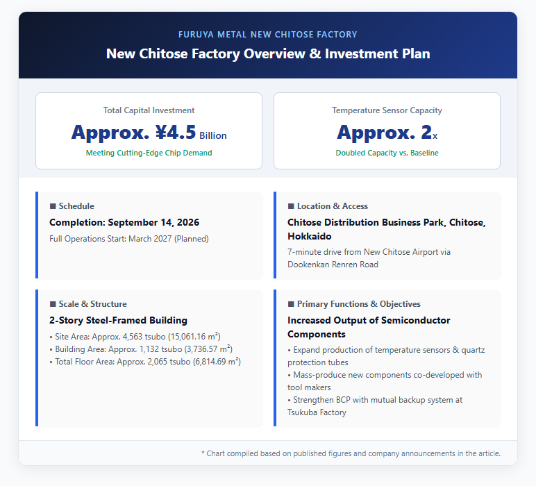
On September 14, 2026, Furuya Metal Co., Ltd. held a completion ceremony for its New Chitose Factory, located within the Chitose Distribution Business Park in Chitose City, Hokkaido. Built with a total capital investment of approximately 4.5 billion yen, the new plant is scheduled to begin full-scale commercial operations in March 2027. At the ceremony, President Takami Furuya highlighted the high expectations from semiconductor manufacturing equipment makers and expressed strong determination to reliably capture expanding market demand.
The New Chitose Factory spans a site area of approximately 4,563 tsubo (15,061.16 m²), with a building area of about 1,132 tsubo (3,736.57 m²) and a total floor area of roughly 2,065 tsubo (6,814.69 m²) across two steel-framed stories. It offers exceptional logistical convenience, situated just a seven-minute drive from New Chitose Airport via the Dookenkan Renren Road.
The primary objective of the facility is to significantly expand the production lines for temperature sensors and high-purity quartz protection tubes used in semiconductor manufacturing equipment—products previously manufactured at the existing Chitose Factory. Once operational, the new site is expected to double Furuya Metal’s production capacity in this sector compared to current levels. For a visual overview of the new facility and its geographical advantages, please refer to the image below.
Role in Chitose’s Emerging Semiconductor Cluster and Joint Product Development
Chitose City, Hokkaido, where the new factory is located, is rapidly evolving into a major industrial cluster for semiconductors, catalyzed by projects such as Rapidus Corporation’s construction of a next-generation chip plant. Establishing this new base in the Chitose Distribution Business Park strengthens Furuya Metal’s geographical integration with nearby advanced chip manufacturing hubs and equipment makers, significantly enhancing supply responsiveness and customer support.
At the New Chitose Factory, initiatives extend beyond increasing the output of existing products, such as temperature sensors and quartz processing products (adding 1,700 new quartz items per year and 4,000 quartz protection tubes for existing thermocouples annually). Specifically, the company plans to mass-produce new products developed jointly with major domestic semiconductor equipment manufacturers.
A key example includes thermal control components designed to dramatically improve heat efficiency in diffusion furnaces, where high-quality oxide films are formed and grown on silicon wafer surfaces at extreme temperatures exceeding 1,000°C. In cutting-edge semiconductor fabrication processes, precise thermal management is indispensable due to relentless miniaturization. Supplying new components tailored to equipment makers’ exact requirements will play a vital role in directly elevating overall tool performance.
Core Technology Behind High-Reliability Sensors and BCP Enhancements
The Ultra-High Temperature “R-SP Process” and High-Quality Manufacturing Environment
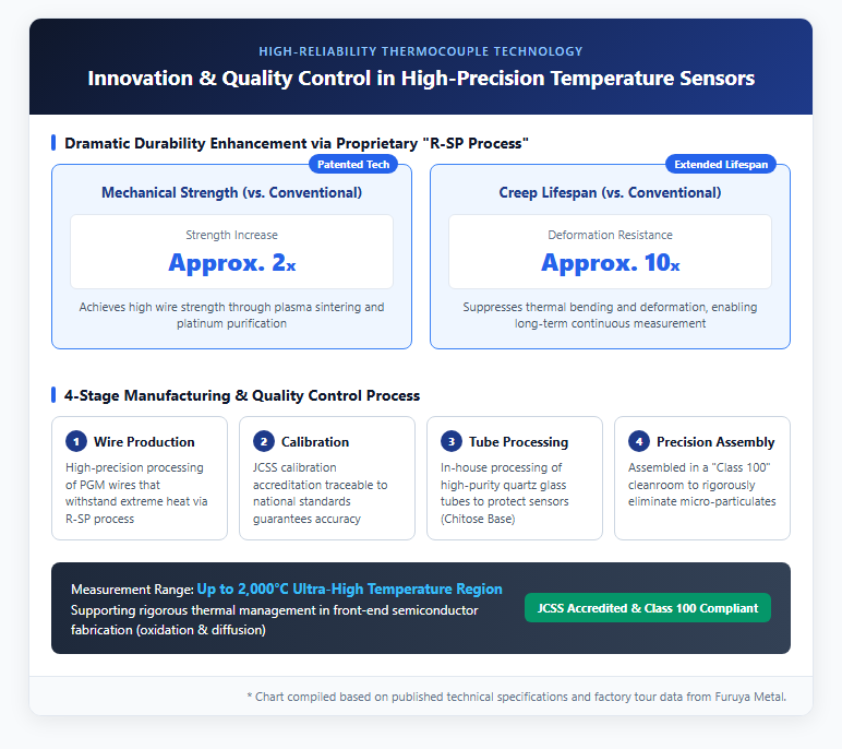
In the oxidation and diffusion steps of front-end semiconductor manufacturing, even minor temperature fluctuations inside a furnace can severely impair product yield and electrical characteristics. Consequently, highly reliable thermocouple sensors capable of continuously and accurately measuring temperatures up to 2,000°C are essential. Furuya Metal possesses world-leading expertise in processing difficult-to-work platinum group metals (PGMs), including platinum, iridium, and ruthenium.
The company’s proprietary “R-SP Process” is an innovative technology that purifies platinum materials to an exceptionally high degree before forming them via plasma sintering. This method achieves approximately double the mechanical strength and ten times the creep resistance (resistance to deformation under high heat) compared to conventional thermocouple wires.
Furthermore, Furuya Metal holds JCSS calibration accreditation, proving traceability to national measurement standards, and assembles its sensors in cleanrooms meeting “Class 100” cleanliness standards to minimize airborne particulates. This rigorous quality assurance infrastructure serves as the foundation for earning immense trust from leading global equipment manufacturers. For a breakdown of the precision sensor assembly process, please refer to the image below.
Strengthening BCP and Supply Stability Through Synergies with the Tsukuba Factory
In response to escalating geopolitical risks and frequent natural disasters in recent years, establishing a robust Business Continuity Plan (BCP) across the semiconductor supply chain has become a paramount priority. With the startup of the New Chitose Factory, Furuya Metal is establishing a dual-production and mutual backup system with its primary facility, the Tsukuba Factory in Chikusei City, Ibaraki Prefecture.
By decentralizing and sharing manufacturing processes and processing capabilities that were previously dependent on a single facility, Furuya Metal is building a sophisticated risk management framework that prevents supply disruptions to customers even in the event of natural disasters or equipment failures.
Additionally, active personnel exchanges of engineers and skilled technicians between both plants will drive process standardization and operational efficiency, boosting overall organizational productivity. Because raw PGM resources are geographically concentrated and globally scarce, maintaining a resilient domestic supply network combined with highly efficient recycling technologies carries profound strategic significance for Japan’s semiconductor industry security.
Future Outlook and Impact on the Semiconductor and AI Industries
Spillover Effects from AI Data Center Demand into Advanced Materials
The expanded production capacity resulting from the completion of the New Chitose Factory will exert a broad ripple effect well beyond the temperature sensor market, benefiting the rapidly growing AI and electronics industries as a whole. As generative AI adoption accelerates, investment in data centers is surging, driving a sharp increase in demand for ruthenium sputtering targets used in ultra-high-density hard disk drives (HDDs) and crystal growth components for optical communication isolators.
Although Furuya Metal does not manufacture semiconductor chips directly, it supplies essential high-value-added materials across the advanced manufacturing process—ranging from internal semiconductor equipment components and thin-film deposition materials to liners for growing next-generation power semiconductor crystals (Gallium Nitride / GaN).
Positioned as an essential material supplier supporting advanced technologies behind the scenes, Furuya Metal benefits from exceptionally high technical entry barriers and strong competitive advantages rooted in long-standing customer relationships. The full-scale operation of the new plant will serve as a powerful engine driving the expansion of cutting-edge chipmaking and AI infrastructure from a materials perspective.
Operational Timeline and Key Watchpoints
Regarding the upcoming schedule, Furuya Metal will install equipment, conduct trial runs on production lines, and prepare the cleanroom environment at the New Chitose Factory through autumn 2026, aiming for formal operational kickoff in March 2027. A phased transition from the existing Chitose Factory will ensure smooth operations, followed by sample shipments to equipment makers and the sequential acquisition of quality certifications.
Key points to monitor moving forward include, first, the ramp-up speed and adoption rate of new thermal control components co-developed with major domestic semiconductor equipment manufacturers. Second, the concrete benefits realized in production efficiency and lead-time reductions through the mutual BCP backup integration with the Tsukuba Factory.
While keeping a close eye on external risks such as volatile PGM market prices and foreign exchange fluctuations, Furuya Metal’s strategic shift toward high-value-added products and the doubling of its stable supply capacity are expected to solidify its long-term growth foundation.
Reference Pages
- [Furuya Metal Co., Ltd. New Chitose Factory Special Site] https://www.furuyametals.co.jp/new-chitose/
- [Furuya Metal Co., Ltd. Press Release (PR TIMES)] https://prtimes.jp/main/html/rd/p/000000009.000097131.html
【#FuruyaMetal #Semiconductors #TemperatureSensors #NewChitoseFactory #PGM #AdvancedTechnology #BCP #ElectronicMaterials】


コメント