
Under Elon Musk’s massive semiconductor manufacturing initiative, “TeraFab,” plans have been revealed to launch a large-scale mass-production plant in Texas in 2032. Behind the complete in-house production of the semiconductors that will support the growth of his corporate group is the aim to overcome the supply constraints of existing foundries and seize leadership in the autonomous driving and AI businesses.
- Key Points of the Initiative and Investment Scale for Mass Production in 2032
- Pushing Development Speed to the Absolute Limit Through a Vertically Integrated Model
- Semiconductor Demand Connecting Autonomous Driving, Robotics, and Space AI
- Geopolitical Risks in Supply Chains and Breaking Away from External Dependence
- Technical Barriers Surrounding 2nm Mass Production and the Debate Over Eliminating Clean Rooms
- Future Outlook and Ripple Effects on the Global Semiconductor Market
Key Points of the Initiative and Investment Scale for Mass Production in 2032
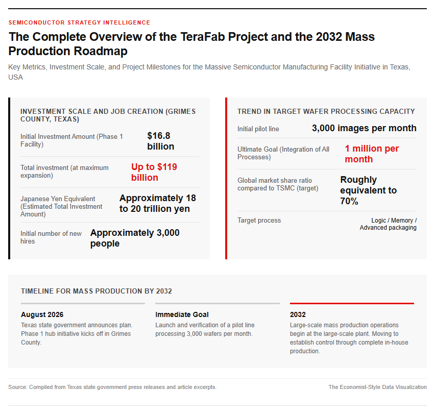
American entrepreneur Elon Musk’s in-house semiconductor manufacturing project, “Terafab,” aims to begin mass production at a large-scale plant in Texas, USA, in 2032. According to a plan announced by the State of Texas in August 2026, the first-phase facility planned for Grimes County, Texas, will receive an initial investment of over $16.8 billion, with an estimated 3,000 new jobs created. Furthermore, total investment including future expansion plans is projected to reach up to $119 billion (approximately 18 trillion to 20 trillion yen). This initiative aims to be more than just a semiconductor assembly plant, striving to become a massive manufacturing hub that consolidates all processes—ranging from advanced logic semiconductor manufacturing to memory and advanced packaging—within a single facility. Toward full-scale mass production in 2032, work is currently underway to launch a pilot line capable of processing 3,000 wafers per month, with an ultimate target processing capacity of 1 million wafers per month, rivaling about 70% of TSMC’s global production capacity. Please refer to the following structure for an overview and timeline of Terafab.
Pushing Development Speed to the Absolute Limit Through a Vertically Integrated Model
The defining characteristic of TeraFab lies in the fully vertically integrated management and production model jointly advanced by Tesla, SpaceX, and xAI. In the conventional semiconductor industry, the dominant structure has been a division of labor between fabless companies that design chips and foundries (contract manufacturers) that specialize in production. However, when outsourcing prototyping and manufacturing to external companies, it takes anywhere from several months to over 18 months from design changes to the completion of prototypes, which has been a factor slowing down the overall product development speed. To address this structural challenge, Musk has proposed an approach that completes everything on the same site—from chip design, the front-end process of wafer circuit formation, and the back-end packaging process, to final verification testing. Through this vertical integration, the aim is to shorten the development feedback loop and compress the chip design revision cycle, which typically takes 18 to 24 months, down to approximately 9 months. By establishing a system that allows hardware to be updated on a monthly basis in tandem with the rapid evolution of software, the goal is to create an overwhelming difference in development speed compared to competitors.
The Managerial and Strategic Background Behind Choosing In-House Manufacturing
Semiconductor Demand Connecting Autonomous Driving, Robotics, and Space AI
At first glance, the diverse businesses involving Elon Musk span a wide range of industries—automobiles, space exploration, AI, and telecommunications—yet all of them share high-performance AI semiconductors as a common core. At Tesla, mass production looms for the “AI5” and “AI6” chips that power next-generation Full Self-Driving (FSD), alongside the “Cybercab” robotaxi and the “Optimus” humanoid robot. In particular, a single humanoid robot requires semiconductors with 10 to 100 times the processing power of an automobile. Furthermore, xAI’s ultra-large supercomputer, “Colossus,” is planned for expansion to a 2-gigawatt scale, consuming massive amounts of computing resources. Additionally, at SpaceX—in addition to rolling out Starlink Mobile services—there are plans to build an in-orbit AI data center equipped with “D3,” a specialized chip capable of withstanding radiation in outer space. In the face of this rapidly expanding demand, the volume of cutting-edge chips currently supplied globally is said to account for only about 3% of the total requirements across all of Musk’s ventures, making the securement of semiconductors itself the single biggest bottleneck hindering the expansion of his businesses.
Geopolitical Risks in Supply Chains and Breaking Away from External Dependence
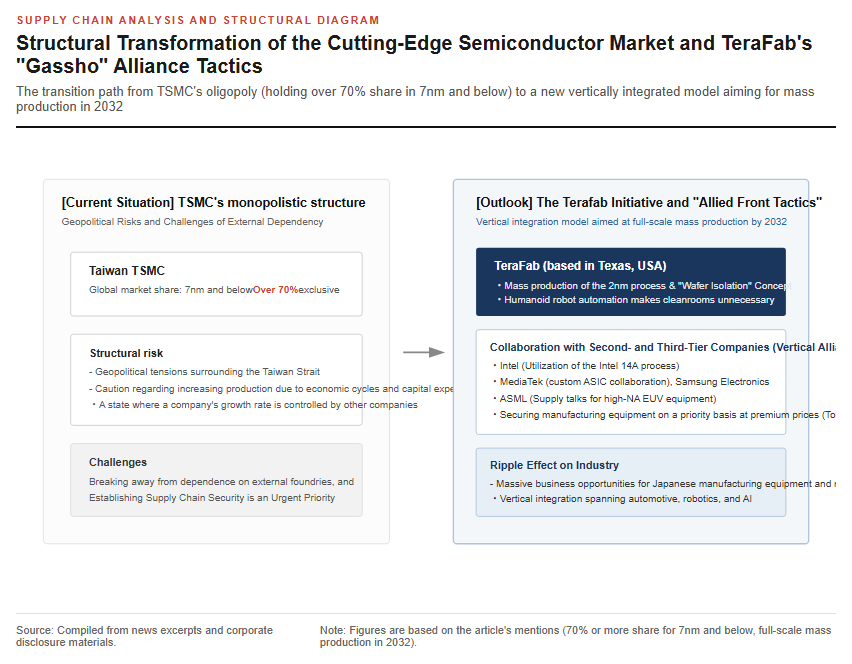
In the global production of cutting-edge semiconductors of 7nm and below, Taiwan’s TSMC continues to hold an exclusive position, commanding over 70% of the global market share. However, rising geopolitical tensions around the Taiwan Strait and the risk of international supply chain fragmentation are life-or-death issues for companies dependent on advanced technology. Major external foundries remain cautious, maintaining a conservative pace of production increases in response to sudden surges in demand due to concerns over economic cycle risks and the massive burden of capital expenditures. Mr. Musk views the situation where his company’s AI evolution and product shipments are restricted by the production capacity and policies of external manufacturers as “having the company’s growth rate controlled by others,” and is seeking to establish supply chain security by setting up his own facility in Texas, USA. Breaking away from dependence on existing suppliers and securing an in-house manufacturing base that avoids geopolitical risks serves as a safety net against future semiconductor supply disruptions, while also acting as a powerful strategic card to extract favorable pricing and delivery terms in negotiations with contract manufacturing companies.
Challenges to Implementation and Future Impact on the Industry
Technical Barriers Surrounding 2nm Mass Production and the Debate Over Eliminating Clean Rooms
The biggest obstacle facing the Terafab concept is the technical difficulty and unique manufacturing approach associated with the mass production of the unchartered 2nm process. Criticizing the conventional cleanroom method of purifying the air in an entire massive facility as inefficient, Musk has proposed a “wafer isolation” concept that keeps only sealed containers or the interior of equipment clean through methods such as nitrogen filling. The rationale is that by automating the entire process with humanoid robots and eliminating humans—the source of dust generation—from the work floor, the air conditioning requirements for the building itself can be relaxed, drastically reducing construction costs and power consumption. However, in the 2nm region where atomic-level microfabrication is performed, slight chemical or humidity fluctuations can catastrophically destroy the yield (the percentage of good products), leading many industry experts to express skepticism about the difficulty of securing yield. To address these challenges, Terafab’s personnel are moving to secure priority access to manufacturing equipment by offering global leading semiconductor manufacturing equipment makers such as Tokyo Electron, Applied Materials of the U.S., and Lam Research price terms that exceed market rates. While they have launched a strategy of buying time with massive funds, the focal point will be whether they can overcome their lack of process launch know-how.
Future Outlook and Ripple Effects on the Global Semiconductor Market
Aimed at full-scale mass production in 2032, TeraFab is deploying an “alliance strategy” to challenge TSMC’s monopoly by uniting second- and third-tier semiconductor companies—utilizing U.S. Intel’s “Intel 14A” process, collaborating on custom ASICs with Taiwan’s MediaTek, and cooperating with Samsung Electronics. Dutch lithography giant ASML has also acknowledged discussions with Musk, and preparations are underway, including the supply of High-NA EUV systems. If even a portion of this project is realized, demand for cutting-edge packaging and 3D stacking technologies will surge, bringing massive business opportunities to Japanese semiconductor manufacturing equipment makers and material manufacturers of silicon wafers and resists, who boast high technological capabilities. Meanwhile, as SpaceX disclosed in its IPO-related documents, there are clear and undeniable risks, such as massive capital expenditure risks, a shortage of specialized talent, and the risk that the project may not succeed as originally intended. Whether TeraFab can upend the conventional wisdom of semiconductor manufacturing by 2032 and establish a vertically integrated model spanning automotive, robotics, and AI is being closely watched by global industries, with a focus on future equipment procurement trends and yield results on the pilot line. The correlation diagram of the semiconductor supply chain is as follows.
Reference page
- [Official State of Texas Announcement (Terafab Construction Project)] https://gov.texas.gov/news/post/governor-abbott-announces-spacex-expansion-in-grimes-county
- [SpaceX Official Announcement (Starship & Communications Business Update)] https://www.spacex.com/updates/starship-moon-announcement
【#TeraFab #ElonMusk #Semiconductors #Tesla #SpaceX #TSMC #AISemiconductors #SupplyChain】
コメント