Microsoft has announced “Azure Maia 300,” its next-generation in-house semiconductor designed for AI inference. By deploying it on a multi-gigawatt scale starting in 2027, the company aims to accelerate its breakaway from NVIDIA dependence and reform the cost structure of its large-scale cloud operations.
- Key Points of Large-Scale Deployment and Technological Evolution Aimed for 2027 Rollout
- Hardware Design Innovations Seen in TSMC 2nm Adoption and HBM4 Integration
- Vertical Integration Strategy Aiming to Cut Costs and Break Away from “NVIDIA Dependency”
- The Impact on Business Performance Brought by Cloud Profitability and Unit Cost Reduction
- The Competitive Landscape of Custom Accelerators Among the Three Major Cloud Providers
- Geopolitical Bottlenecks in Advanced Semiconductor Manufacturing and HBM Procurement, and Key Areas to Watch
Key Points of Large-Scale Deployment and Technological Evolution Aimed for 2027 Rollout
On October 12, 2026, Microsoft announced “Azure Maia 300,” its next-generation proprietary accelerator specialized for artificial intelligence (AI) inference processing. The company plans to begin large-scale deployments totaling several gigawatts in scale starting in 2027 across data centers worldwide, including in the United States. This chip is positioned as core infrastructure supporting key services such as the conversational AI “Microsoft Copilot,” “GitHub Copilot,” and the enterprise development platform “Microsoft Foundry,” and will be rolled out sequentially to global locations, including Japan.
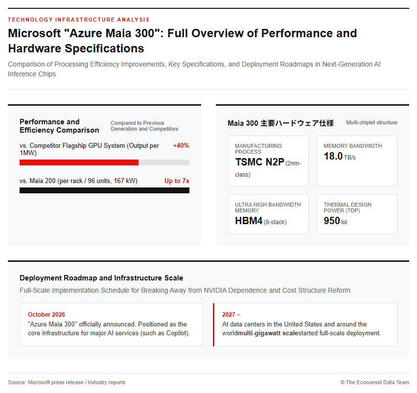
While the previous-generation “Maia 200” achieved up to 1.7 times the processing efficiency per unit of power as the infrastructure for Teams and Copilot, the Maia 300 dramatically boosts processing performance per watt. Compared to competing flagship GPU systems, it enables a 40% increase in token output per megawatt, and on a rack basis (equipped with 96 units, consuming 167 kilowatts), it delivers processing capacity up to 7 times that of the Maia 200. As the operational scale of AI models expands dramatically, the approach of maximizing output per unit of power has become a crucial technological advancement in addressing data center power supply constraints.
Hardware Design Innovations Seen in TSMC 2nm Adoption and HBM4 Integration
Supporting the exceptional power efficiency of the Azure Maia 300 is a multi-chiplet structure utilizing the advanced “N2P” (2-nanometer class) process from semiconductor foundry giant TSMC. By separating and integrating computing, memory control, and input/output functions into individual chiplets, it achieves both high manufacturing yields and cost optimization. Furthermore, it is equipped with eight stacks of “HBM4,” an ultra-high-bandwidth memory module (providing a total memory bandwidth of 18.0 TB/s), enabling high-speed processing of massive AI models within a 950-watt thermal design power (TDP) envelope. The following diagram illustrates the complete internal architecture of the Maia 300.
Another notable feature is that, unlike conventional general-purpose GPU architectures, it adopts a software-defined dataflow structure that eliminates data movement bottlenecks. By utilizing the on-die SRAM inside the chip as scratchpad memory and reducing the access load on expensive HBM, it minimizes power loss caused by data movement. In addition, through the optimization of the “MXFP4” low-precision format and the introduction of a high-bandwidth interconnect based on Ethernet technology, it achieves dramatic improvements in response speed for understanding complex long-text contexts and the continuous processing of autonomous AI agents.
The Background and Economic Incentives Behind Big Tech’s Rush to Develop In-House Chips
Vertical Integration Strategy Aiming to Cut Costs and Break Away from “NVIDIA Dependency”
The primary factor driving major cloud service providers to invest massive amounts of capital into developing proprietary silicon (ASICs) lies in the high-cost structure and supply constraints of NVIDIA GPUs, which dominate the AI computing market. With the proliferation of generative AI, a shift in demand for computing resources has occurred from the model training stage to “inference,” which takes place during actual service operations, and inference processing now accounts for approximately 60% to 80% of AI-related computing costs. In inference, where large volumes of user requests are processed continuously, the deployment of general-purpose GPUs leads to high costs, and reliance on the so-called “CUDA ecosystem” has become a factor squeezing profit margins.
To address this challenge, Microsoft has chosen a “vertical integration” strategy, handling everything from semiconductors (Maia) and cloud infrastructure (Azure) to the OS (Windows) and applications (Copilot) entirely in-house. By optimally designing only the circuits necessary for specific inference workloads and stripping away unnecessary functions, it achieves a cost-performance that surpasses general-purpose chips. Similar initiatives are also being driven by Amazon Web Services (AWS) with Trainium/Inferentia and Google with TPUs, intensifying the battle for hardware supremacy among hyperscalers.
The Impact on Business Performance Brought by Cloud Profitability and Unit Cost Reduction
Microsoft’s expansion of its proprietary chips is acting as a direct tailwind for improving the profitability of its cloud business, Microsoft Azure. According to the company’s fourth-quarter earnings for fiscal year 2026, Azure’s revenue growth accelerated to 43% year-over-year, and cloud-related order backlog reached a record high of $678 billion (approximately 106.8 trillion yen), an 84% increase from the previous year. While demand for AI services continues to grow, reducing capital expenditures (CapEx) and electricity costs associated with establishing and operating data centers has become a top management priority. The following graph illustrates the trend in infrastructure cost reduction effects resulting from the deployment of proprietary chips.
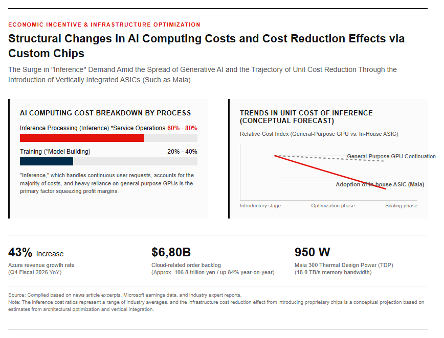
When running customized proprietary large language models, such as “MAI,” on proprietary semiconductors, a 40% improvement in performance per watt has been confirmed compared to general-purpose chips. In a cloud infrastructure that executes inference processing across a server fleet numbering in the millions, improved processing efficiency per unit of electricity translates to a dramatic reduction in token unit costs (response generation costs). This unit cost improvement enables competitively priced enterprise AI services, making it possible to simultaneously sustain high capital expenditure burdens while expanding mid- to long-term free cash flow and securing high profit margins.
Future Prospects of AI Infrastructure and Geopolitical Risks in the Supply Chain
The Competitive Landscape of Custom Accelerators Among the Three Major Cloud Providers
Competition in the AI hardware market has evolved beyond mere differences in individual chip performance into a struggle for dominance that involves entire cloud service ecosystems. The proprietary silicon lineups of the three major cloud providers—Microsoft’s “Azure Maia,” AWS’s “Trainium / Inferentia,” and Google’s “TPU”—are not rented out individually to external cloud environments; instead, they are operated exclusively as computing resources within their respective cloud platforms. For enterprise users, this creates a structure where the choice of cloud provider determines the specifications and cost-effectiveness of the proprietary semiconductors they can utilize.
In this competition, Microsoft is leveraging open-source software such as Triton to rapidly build an open development ecosystem that rivals NVIDIA’s flagship “CUDA” programming environment. By preventing developers from being “locked in” to a specific hardware vendor and offering an environment where models can be flexibly optimized across multi-architectures, it is enhancing the appeal of Azure. Leveraging its track record with in-house applications (such as Copilot), the company is advancing its differentiation as a platform capable of efficiently running everything from open models to proprietary models.
Geopolitical Bottlenecks in Advanced Semiconductor Manufacturing and HBM Procurement, and Key Areas to Watch
While in-house chip development is accelerating, deep-seated geographical and structural concentration risks remain within the AI semiconductor supply chain. TSMC’s advanced fabs responsible for manufacturing the Maia 300 are concentrated in Taiwan, and reliance on the Netherlands’ ASML, which has a monopoly on the supply of advanced lithography equipment, is unavoidable. Furthermore, the market for HBM (High Bandwidth Memory), which is essential for high-performance processing, is under a tight oligopoly by just three companies—South Korea’s SK Hynix and Samsung Electronics, and U.S.-based Micron Technology—causing ripple effects such as tight supply and demand across entire memory modules that drive up prices for general-purpose DRAM.
In addition, China’s near-monopoly on the refining capacity of critical minerals such as gallium, germanium, and rare earth elements remains a stubborn bottleneck that is difficult to resolve in the short term, even with U.S. efforts to bring domestic manufacturing back through the CHIPS Act. Moving forward, the greatest points of focus—which will dictate the growth rate of the AI infrastructure market and the direction of global supply chain restructuring—will be the progress of local production at TSMC Arizona and elsewhere ahead of the full-scale deployment of the Maia 300 in 2027, the securing of multi-gigawatt-scale power, and trends in export controls driven by the U.S.-China conflict.
Reference page
- [The Official Microsoft Blog] https://blogs.microsoft.com/blog/2026/10/12/microsoft-to-expand-azure-maia-system-to-multi-gigawatt-deployments/
[#Microsoft #AISemiconductor #AzureMaia300 #NVIDIA #CloudBusiness #InHouseChip #TSMC]


コメント