
Tamron has succeeded in the practical application of a heat-resistant chip-type “Metasurface Near-Infrared Light Source Using MIM Structure” through joint research with Osaka University. By applying thermal management technology cultivated over many years of lens manufacturing, we enable dramatic miniaturization and power savings in analytical instruments.
- Key Points of the Announcement and Development Background
- Innovations Brought by MIM Structures and Metasurfaces
- Unexpected Adaptation of GM Lens Manufacturing Technology
- Outstanding performance figures that withstand harsh environments
- The Industrial Revolution Driven by Handheld Analytical Instruments
- Future Developments and Highlights
Key Points of the Announcement and Development Background
On June 19, 2026, Tamron Corporation announced that, through joint research with Professor Junichi Takahara of Osaka University, it has successfully commercialized the world’s first chip-type “metasurface near-infrared light source using MIM structure” with excellent heat resistance. This news is important because it holds the potential to evolve previously large and expensive near-infrared analyzers into portable sizes as easily as smartphones.
Traditional analysis and inspection equipment has used lamps as light sources, but these have had the critical drawback of emitting unwanted wavelengths, resulting in energy loss and significant heat generation. Cooling devices to dissipate this heat were necessary, which typically resulted in the entire equipment becoming larger and heavier. However, the newly commercialized light source can precisely transmit only the required wavelength, achieving both significant power savings and downsizing simultaneously. With this technology, Tamron plans to begin offering commercial samples in autumn 2026, aiming for full-scale social implementation and market launch.
Innovations Brought by MIM Structures and Metasurfaces
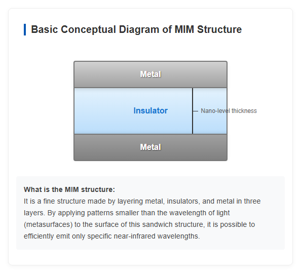
The key to practical application this time, the “MIM (Metal-Insulator-Metal) structure,” refers to an extremely fine structure at the nanometer level, made by stacking metal, insulators, and metals in three layers. By applying microstructures called “metasurfaces,” smaller than the wavelength of light, to the surface, it becomes possible to freely control the properties of light and electromagnetic waves. Specifically, it can function as a “wavelength-selective thermal emitter” that efficiently emits only infrared radiation of specific wavelengths.
This structure has the major advantage of being thin and lightweight, but the biggest barrier to practical application was “heat.” To achieve high radiation intensity, the luminous source must be kept at temperatures of several hundred degrees, but conventional materials and structures could not avoid rapid degradation due to this heat. If the precise structure of nanometers physically breaks down due to high temperatures, the crucial function of producing specific wavelengths is lost. Due to this technical dilemma, the social implementation of MIM-structured light sources has long been considered difficult, but Tamron has tackled and successfully overcome this challenge from its unique perspective. The diagram below illustrates the basic units of the MIM structure and its concepts.
Tamron’s unique approach breaks through the heat barrier
Unexpected Adaptation of GM Lens Manufacturing Technology
Surprisingly, what Tamron leveraged to solve the challenge of thermal degradation was the technology cultivated at the manufacturing sites of its core camera lens business. Specifically, we applied the expertise accumulated over many years in heat treatment and thermal management during the manufacturing process of “GM (Glass Mold) lenses.” GM lenses are produced by heating the glass material at ultra-high temperatures and pressing them with molds precisely made at the nanometer level. This process requires advanced technology to strictly control heat while maintaining extremely high precision.
Tamron has applied this unique technology of “highly controlling heat” to light source development, establishing a unique manufacturing process that maintains structural damage and continues to emit light stably even under high thermal loads. The foundational technologies honed over many years of history as an optical manufacturer played a decisive role in developing next-generation light sources, which are a completely different field. This event symbolized the company’s evolution from “photography technology” to “measurement technology,” and it once again demonstrated the company’s outstanding technical strength that connects basic research to mass production.
Outstanding performance figures that withstand harsh environments
Looking at the performance figures of the practical light source, its overwhelming reliability becomes apparent. The light emitter covers an extremely high operating temperature range from 400°C to 800°C, and even during continuous light at 500°C, it guarantees a lifespan of over 1,000 hours. Notably, even when the luminous material itself reaches a high temperature of 500°C, the surface temperature of the device remains 85°C without cooling, and when combined with weak air cooling, it can be kept down to about 50°C, demonstrating its thermal insulation performance.
Furthermore, its power consumption at 500°C is only 1.5W. This represents a dramatic power reduction compared to conventional lamp-type light sources, making installation in battery-powered portable inspection equipment completely feasible. Additionally, the device itself is set at a heat resistance temperature of 250°C, making it robust enough to withstand factory production lines and harsh outdoor environments. Because it uses a common drive method of DC power supply and constant current control, it is extremely easy to integrate into existing electronic circuits. In this way, the strength of this technology lies in achieving extremely practical specifications that go beyond laboratory-level theoretical values, assuming integration into actual products.
The spread of ‘measuring’ technologies that change society
The Industrial Revolution Driven by Handheld Analytical Instruments
The social significance brought by this handy-sized near-infrared light source is wide-ranging. First, in the beauty and healthcare sectors, the emergence of smartphone-linked devices that can precisely measure skin condition and blood flow on the spot is anticipated. A future is approaching where advanced analyses that previously required visiting hospitals or specialized institutions can now be easily performed at home or in stores.
Additionally, their contributions to the food and agriculture sectors are significant. For example, since fruit sugar content, moisture, and lipid content can be measured instantly without destructiveness, accurate harvest timing determination and quality control at shipment become dramatically more efficient. By combining with existing technologies such as SWIR (shortwave infrared light) lenses that Tamron has already deployed, it will be possible to provide more advanced sensing solutions for agriculture. Furthermore, at infrastructure inspection sites such as structural deterioration diagnosis of buildings and bridges, there is no longer a need to bring heavy analytical equipment, which is expected to reduce the workloader on workers and increase inspection frequency. In today’s world, where everything is connected to the internet, this “chip-shaped eye” is expected to become an extremely important interface for instantly digitizing information from the physical world.
Future Developments and Highlights
As a concrete future schedule, Tamron plans to hold a lecture and actual display of this technology at the “Infrared Array Sensor Forum 2026,” held at Ritsumeikan University on July 3, 2026. By sharing technical details with experts and industry and showcasing actual samples, the goal is to gather feedback for the final stages toward practical application.
Starting in autumn 2026, we will begin offering commercial samples to companies and research institutions wishing to try them, accelerating partnerships for concrete next-generation product development. Tamron has set forth its long-term vision: “Shoot, measure, connect. A company that creates the health of people and nature,” and the practical application of next-generation light sources this time marks a symbolic step that embodies that vision. The company’s transformation beyond being a specialized lens manufacturer into a “comprehensive optics and sensing solutions company” integrating AI, image processing, and advanced sensing technologies will continue to attract significant attention.
[#タムロン #次世代光源 #メタサーフェス #近赤外線 #光学技術 #大阪大学 #非破壊検査 #赤外線センサ]
コメント