
Driven by an exponential surge in demand for High Bandwidth Memory (HBM) used in AI semiconductors, Micronics Japan Co., Ltd. (MJC) achieved a remarkable milestone, doubling its operating profit year-over-year in its fiscal first-half ending June 2026. This explosive growth was enabled by MJC’s strategic, proactive investments in expanding production capacity, highlighted by the construction of a new building at its Aomori Factory.
- Exploding Net Sales and Operating Profit in H1 FY2026
- Core Probe Card Business Drives High-Margin Revenue Structure
- Upward Revision of Full-Year Outlook Validates Proactive Capital Allocation
- Ultra-Precise Testing Processes as the Key Bottleneck in AI Semiconductors
- The Three Technical Hurdles and the Superb Edge of MEMS Probe Cards
- Strategic Alliance with Advantest for Next-Generation Test Solutions
- Production Expansion and Key Growth Metrics to Watch
Exploding Net Sales and Operating Profit in H1 FY2026
On August 12, 2026, Micronics Japan Co., Ltd. (MJC) announced its consolidated financial results for the first half of the fiscal year ending December 31, 2026. Net sales surged to 49,206 million yen, representing a robust 48.6% increase year-over-year, while operating profit skyrocketed by an astonishing 105.5% to 15,557 million yen, more than doubling from the previous year. Ordinary profit grew by 119.9% to 16,260 million yen, and net income attributable to owners of the parent leaped by 140.0% to 11,461 million yen. This stellar performance is primarily powered by the rapid proliferation of generative AI and aggressive datacenter investments by hyperscale cloud service providers. The skyrocketing demand for advanced logic chips, such as GPUs, alongside high-capacity High Bandwidth Memory (HBM), has heavily driven the semiconductor market. As major memory manufacturers prioritized HBM and high-value-add server products over general-purpose DRAM, the supply-demand balance for standard DRAM tightened, pushing market prices upward and significantly boosting MJC’s top and bottom lines. Furthermore, the NAND flash market showed a clear recovery trend, driven by growing demand from datacenters and ongoing supply adjustments, providing strong additional support to MJC’s earnings.
Core Probe Card Business Drives High-Margin Revenue Structure
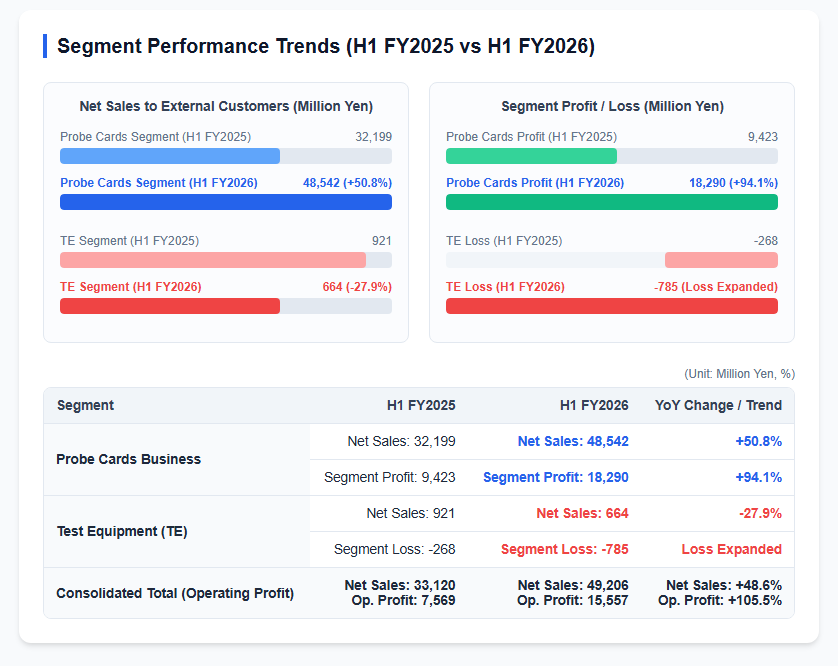
The powerhouse behind MJC’s profitability is its probe card business, which produces essential testing components used in wafer-level semiconductor testing. In the first half of FY2026, the probe card segment recorded net sales of 48,542 million yen, a 50.8% increase year-over-year, and segment profit of 18,290 million yen, a massive 94.1% increase. This business alone accounts for more than 98% of the company’s total net sales, showcasing a highly concentrated yet robust product portfolio. The key driver was the outstanding performance of DRAM probe cards, coupled with an increasing ratio of high-margin, advanced probe cards for HBM stack devices, which significantly elevated overall profitability. In contrast, the company’s other business, Test Equipment (TE), saw its net sales decrease by 27.9% to 664 million yen. Hampered by heavy upfront research and development expenses, the TE segment registered a loss of 785 million yen, expanding its deficit from the 268 million yen loss in the same period last year. While the TE business continues to face a challenging environment, the exceptional earnings power of the probe card segment dominantly steers the company’s upward trajectory.
The following table displays the transition of net sales and segment profits/losses for each business segment during the first half.
Upward Revision of Full-Year Outlook Validates Proactive Capital Allocation
Building on its spectacular first-half momentum, MJC significantly revised its full-year consolidated earnings forecast for the fiscal year ending December 31, 2026. The revised outlook projects full-year net sales of 103,800 million yen (up 47.9% year-over-year) and an operating profit of 31,400 million yen (up 89.8% year-over-year), reaching a stellar operating margin of approximately 30%. This massive growth is the direct result of MJC’s aggressive capital allocation executed ahead of the demand spike. Between 2023 and 2026, the company poured tens of billions of yen into capital expenditures and R&D, notably building a state-of-the-art facility at its Aomori Factory. This strategic capacity expansion aligned perfectly with the explosive demand for DRAM and HBM sparked by the generative AI boom, translating immediately into top-line revenue. First-half earnings per share reached 295.65 yen, a dramatic jump. Backed by this financial strength, the company announced an upward revision to its full-year dividend forecast from the previously planned 95 yen to 178 yen per share—nearly doubling its shareholder return and highlighting a strong commitment to sharing its financial success.
The HBM Era Sparks a Surge in Probe Card Demand
Ultra-Precise Testing Processes as the Key Bottleneck in AI Semiconductors
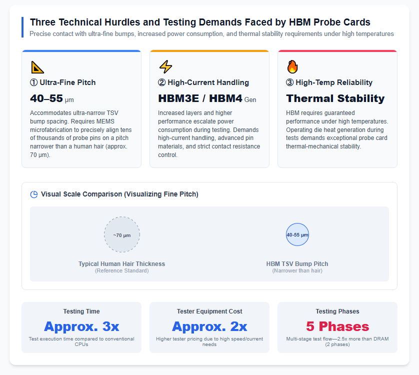
To maximize the performance of AI processors, high-speed and high-capacity HBM is indispensable. However, HBM manufacturing is incredibly complex, with yield rates acting as the primary bottleneck in mass production. Because HBM requires multiple DRAM chips to be stacked vertically, manufacturers must conduct meticulous testing of individual dies before stacking—a process known as securing Known Good Dies (KGD). If even a single defective die is incorporated into a stack, the entire multi-layered stack becomes useless, resulting in catastrophic material losses. Consequently, HBM testing requires more than twice the process steps of standard DRAM. The total testing time for AI processors can be up to three times longer than that of traditional CPUs, while the cost of advanced testing equipment has nearly doubled. This intense testing requirement has created an unprecedented demand for probe cards, the critical interface connecting the testing equipment to the semiconductor wafers.
The Three Technical Hurdles and the Superb Edge of MEMS Probe Cards
HBM probe cards are subjected to technical requirements far more stringent than conventional products. Specifically, they must overcome three major technical hurdles. First, they require the ultra-precise alignment of tens of thousands of microscopic pins onto an extremely narrow pitch of 40 to 55 micrometers—matching the microscopic Through-Silicon Via (TSV) bumps, which are much thinner than a human hair (approximately 70 micrometers). Second, to handle the escalating power consumption in HBM3E and next-generation iterations, the probe cards must manage high electrical currents during testing, requiring specialized pin materials and precise control of contact resistance. Third, they must possess exceptional thermal-mechanical stability, ensuring the pin tips do not drift despite the extreme heat generated by the active dies during testing. To bypass these barriers of fine-pitch, high-current, and high-heat, manufacturers rely on MEMS (Micro-Electro-Mechanical Systems) probe cards, fabricated using semiconductor photolithography to batch-form micro-needles on substrate materials. MJC’s signature products leverage state-of-the-art MEMS engineering, erecting a high barrier of entry that rivals cannot easily duplicate.
The diagram below illustrates the fundamental requirements and parameters of MEMS-based HBM probe testing.
Competitive Edge and Mid-to-Long Term Global Strategy
Strategic Alliance with Advantest for Next-Generation Test Solutions
On February 27, 2025, MJC announced a landmark strategic partnership with Advantest Corporation, the world’s leading manufacturer of semiconductor automatic test equipment (ATE). As chip-testing processes grow increasingly complex, the alliance unites the dominant player in testing systems with a leader in probe card technology. The goal is to co-develop high-performance, comprehensive test solutions leveraging each other’s specialized expertise. As part of this alliance, Advantest acquired 150,000 shares of MJC’s treasury stock via a third-party allotment, providing MJC with approximately 620.4 million yen in funding. This capital is entirely designated for research and development to establish cutting-edge technology for next-generation semiconductor test solutions. Because testing systems and probe cards must operate in perfect unison to be effective, this strategic synergy acts as a major catalyst, positioning both companies to establish an unrivaled competitive advantage in tackling high-difficulty testing requirements.
Production Expansion and Key Growth Metrics to Watch
MJC’s long-term sustainability hinges on keeping its expanded capacity—particularly the new facilities at the Aomori Factory—running at high utilization rates while maintaining its impressive 30% operating margin. Although the global HBM market is projected to expand at an exponential compound annual growth rate (CAGR) of over 52% from 2023 to 2027, the company must navigate macroeconomic fluctuations, trade tensions between the US and China, and potential sales concentration risks among key customers. To mitigate these risks, MJC maintains close technical collaborations with key clients, preparing to launch next-generation products aligned with future roadmaps, including HBM4. Additionally, MJC is actively leveraging its dominant memory probe technology to penetrate the non-memory (logic) testing market, a sector currently dominated by competitors like FormFactor. Successful portfolio diversification into logic testing will serve as a crucial milestone for maximizing MJC’s enterprise value in the mid-to-long term.
References
- 【Micronics Japan Co., Ltd. Official Website】https://www.mjc.co.jp/
- 【Advantest Corporation Official Website】https://www.advantest.com/
【#MicronicsJapan #MJC #AISemiconductors #HBM #ProbeCards #FinancialResults #Advantest #Business】


コメント