Chinese memory giant ChangXin Memory Technologies (CXMT) has reportedly begun small-scale production of its cutting-edge High Bandwidth Memory, HBM3E, supplying evaluation samples and conducting adoption testing with Alibaba subsidiary T-Head and AI chipmaker Cambricon. This milestone highlights China’s aggressive strategic push to build a self-sufficient AI semiconductor ecosystem in response to tightening US export controls.
- CXMT Advances HBM3E Development and AI Chip Adoption Testing
- Yields Stagnate at 25% Amid TSV Stacking Challenges
- CXMT and YMTC Form a Strategic HBM Alliance
- Massive Capital Injections from National IC Fund and Local Governments
- Responding to BIS Export Restrictions with Domestic Equipment Integration
- Generational Gap with Global Leaders and Long-Term Market Outlook
CXMT Advances HBM3E Development and AI Chip Adoption Testing
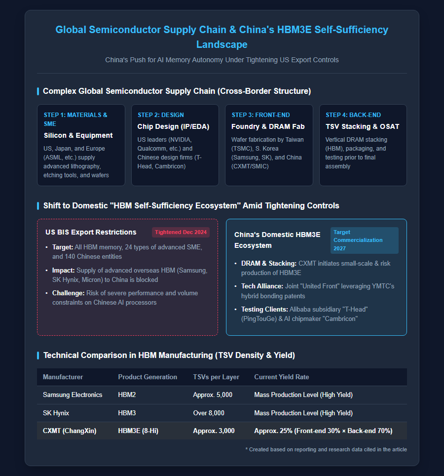
ChangXin Memory Technologies (CXMT), China’s leading DRAM manufacturer, has entered the risk production phase by starting small-scale manufacturing of HBM3E—a high-bandwidth memory critical for artificial intelligence applications. CXMT’s prototype HBM3E chips are currently being supplied as evaluation samples to T-Head (PingTouGe), the semiconductor design arm of Alibaba Group, and Cambricon Technologies, a prominent Chinese AI chipmaker. Both companies are actively conducting adoption tests to evaluate the memory’s integration into their proprietary AI processors, with potential commercial adoption anticipated as early as 2027 if evaluations proceed smoothly. HBM is an advanced memory architecture that vertically stacks DRAM dies connected via Through-Silicon Vias (TSVs), facilitating high-speed data transfer to GPUs and AI accelerators. As the US Department of Commerce’s Bureau of Industry and Security (BIS) tightened export controls on HBM in December 2024, CXMT’s domestic HBM3E supply serves as a critical alternative source for Chinese AI chip manufacturers facing international procurement restrictions. The diagram below illustrates the complex global semiconductor supply chain.
Yields Stagnate at 25% Amid TSV Stacking Challenges
While CXMT’s HBM3E development shows steady progress, low manufacturing yields pose a severe challenge to commercial mass production. According to South Korean media reports, three out of every four HBM3E stacks produced by CXMT are defective, leaving current yields at a mere 25%. This low yield is primarily attributed to immature Through-Silicon Via (TSV) technology used in stacking DRAM dies. Specifically, CXMT achieves a front-end wafer yield of approximately 30%, which drops to a final post-packaging yield of around 25%. A comparison of TSV density among industry leaders highlights the difficulty: while Samsung Electronics deployed roughly 5,000 TSVs per layer for HBM2 and SK Hynix used over 8,000 TSVs per layer for HBM3, CXMT is attempting an 8-layer (8-Hi) HBM3E configuration with only 3,000 TSVs per layer. Although CXMT boasts yields exceeding 90% for conventional planar DRAM like DDR5, mastering 3D stacking technology will require additional time.
China’s “HBM United Front” and State-Backed Ecosystem
CXMT and YMTC Form a Strategic HBM Alliance
To overcome critical packaging and bonding bottlenecks in HBM manufacturing, China’s semiconductor industry has formed an unprecedented cross-company “united front.” CXMT has established a comprehensive partnership with Yangtze Memory Technologies Corp (YMTC), China’s top NAND flash maker, focused on joint HBM development starting in 2025. YMTC holds proprietary patents for advanced “hybrid bonding” technology developed for its 400-layer 3D NAND; integrating this bonding expertise into CXMT’s HBM3E production process aims to dramatically improve yields. Private sector support is equally strong: Alibaba Group, holding approximately a 5% stake in CXMT, uses CXMT DRAM in its data centers and is co-developing HBM3E integration for its proprietary T-Head AI accelerators. Tech leaders like Huawei and Xiaomi are also acting as primary clients, bolstering the domestic semiconductor ecosystem.
Massive Capital Injections from National IC Fund and Local Governments
Underpinning the rapid rise of Chinese semiconductor firms is an unprecedented level of financial backing provided jointly by the central government, local authorities, and financial institutions. Since 2014, Beijing has funneled roughly 680 billion yuan (approx. \$95 billion) through the National Integrated Circuit Industry Investment Fund (known as the “Big Fund”). An examination of CXMT’s ownership structure reveals that local government funds, including the city of Hefei, hold a combined 50% stake, while the Big Fund holds 8.73%. Similarly, YMTC’s parent company, Changjiang Chunchiu Holding, is 70% owned by local government funds and 23.35% by the Big Fund, effectively operating both as state-backed entities. CXMT successfully listed on the STAR Market of the Shanghai Stock Exchange in July 2026, raising 57.9 billion yuan (approx. \$8.6 billion) after institutional demand exceeded supply by 570 times.
Production Capacity Expansion Under US Sanctions and Global Market Impact
Responding to BIS Export Restrictions with Domestic Equipment Integration
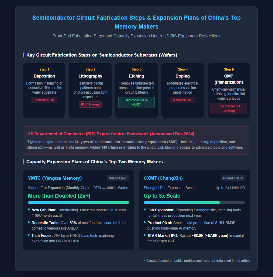
In December 2024, the US Department of Commerce further expanded export controls targeting China, restricting 24 types of semiconductor manufacturing equipment (SME)—including etching, deposition, and lithography tools—as well as HBM, while adding 140 Chinese entities to its Entity List. Blocked from acquiring advanced tools like Extreme Ultraviolet (EUV) lithography machines, Chinese memory makers are aggressively constructing production lines utilizing domestic equipment. NAND giant YMTC is constructing three new fab modules in Wuhan, Hubei Province, each with a monthly capacity of 100,000 wafers, aiming to more than double its total capacity from 200,000 to over 400,000 wafers per month. More than 50% of the equipment installed in these new facilities is sourced from domestic suppliers, including AMEC, China’s leading etching equipment maker. Concurrently, DRAM leader CXMT is expanding its Shanghai facility to build a manufacturing footprint up to three times larger than its Hefei headquarters fab. The diagram below outlines the semiconductor wafer circuit fabrication process.
Generational Gap with Global Leaders and Long-Term Market Outlook
On the global stage, the industry’s top three memory makers—Samsung Electronics, SK Hynix, and Micron Technology—are transitioning to mass production of next-generation HBM4, featuring a 2,048-bit wide interface. As South Korean manufacturers enter full-scale HBM4 production in 2026, CXMT’s commencement of small-scale HBM3E production reflects a technological lag of approximately three years. However, China is rapidly closing the broader memory gap: the DRAM technology gap between South Korea and China has narrowed from five years in 2022 to roughly two years, while YMTC’s 270-layer 3D NAND puts it within a year of South Korean leaders. If China achieves domestic HBM self-sufficiency, it could significantly reduce demand for Korean HBM supplied indirectly via Nvidia and other global vendors, restructuring global memory trade flows. CXMT’s ability to pass customer qualification and establish stable, high-yield volume production remains the pivotal factor shaping the future AI semiconductor supply chain.
Reference Pages
- [U.S. Department of Commerce Bureau of Industry and Security (BIS) Press Release] https://www.bis.gov/press-release/commerce-strengthens-export-controls-restrict-chinas-capability-produce-advanced
【#ChinaSemiconductors #HBM3E #CXMT #YMTC #ExportControls #AIAccelerators #YieldRate #STARMarket】


コメント