
On September 17, 2026, Fujifilm Corporation announced a partnership with India’s Tata Electronics to invest approximately 13 billion yen (around 8 billion rupees) in constructing the nation’s first semiconductor materials plant in Dholera, Gujarat. Aligning with the Indian government’s “Semicon 2.0” initiative, Fujifilm aims to build a resilient, localized supply chain covering everything from raw material sourcing to final manufacturing.
- Two-Phase Investment Plan of ¥13 Billion and Execution Timeline
- Strategic Partnership with Tata Electronics and Strategic Location in Dholera
- Indian Market Expanding to $100 Billion by 2030 and Government Support
- Supply Chain Diversification and the Geopolitical Significance of “China Plus One”
- Adapting Core Photographic Film Technologies to Advanced AI Semiconductor Materials
- Challenges in Establishing a Local Supply Chain and Key Focus Areas Ahead
Two-Phase Investment Plan of ¥13 Billion and Execution Timeline
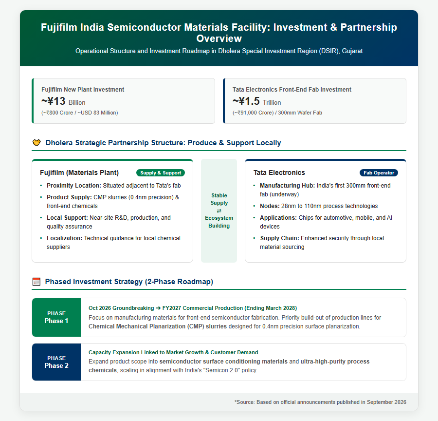
On September 17, 2026, Fujifilm Corporation announced a plan to invest approximately 8 billion rupees (around 13 billion yen or USD 83 million) to establish its first greenfield semiconductor materials manufacturing facility in India. To manage risk effectively while keeping pace with market growth and customer demand, the project adopts a phased investment strategy.
Phase 1 is scheduled to break ground in October 2026, focusing specifically on manufacturing materials used in front-end semiconductor fabrication processes. In particular, production lines will be established for Chemical Mechanical Planarization (CMP) slurries—high-precision polishing agents designed to achieve extreme surface flatness on semiconductor wafers. Facility construction and equipment installation will be fast-tracked to achieve commercial production within fiscal year 2027 (ending March 2028).
Following Phase 1, Phase 2 will expand production capacity to include semiconductor surface conditioning materials and ultra-high-purity process chemicals, scaling in alignment with the growth pace and demand of the Indian semiconductor industry.
Through this landmark project, Fujifilm integrates India into its global manufacturing network—which already spans Japan, the United States, Europe, and East Asia—thereby enhancing its global supply capability and operational resilience.
Strategic Partnership with Tata Electronics and Strategic Location in Dholera
Fujifilm’s new facility will be located in the Dholera Special Investment Region (DSIR) in the western state of Gujarat. Dholera is a premier special economic zone where the Indian government is aggressively building out infrastructure to establish a major national hub for the semiconductor industry.
The decisive factor in selecting this location is Fujifilm’s robust strategic partnership with Tata Electronics Private Limited, a leading domestic electronics manufacturer. Tata Electronics is investing approximately 910 billion rupees (around 1.5 trillion yen) in DSIR to build India’s first 300mm (12-inch) wafer front-end semiconductor fabrication plant. This mega-fab will produce semiconductor chips across 28-nanometer to 110-nanometer process nodes for automotive, mobile, and AI applications.
By constructing its materials plant adjacent to Tata’s front-end fab, Fujifilm will advance three core operational pillars:
- Establishing a localized “produce-for-local” supply system to guarantee stable, uninterrupted delivery
- Implementing a “local support” framework to deliver rapid, close-proximity technical and quality management assistance
- Localizing raw material procurement by providing technical guidance to local Indian chemical suppliers
Dr. Randhir Thakur, CEO and Managing Director of Tata Electronics, emphasized that this strategic collaboration with Fujifilm will dramatically strengthen the security and resilience of Tata’s fab supply chain. Please refer to the following diagram for details.
Rapid Growth of the Indian Semiconductor Market and the “Semicon 2.0” Policy Background
Indian Market Expanding to $100 Billion by 2030 and Government Support
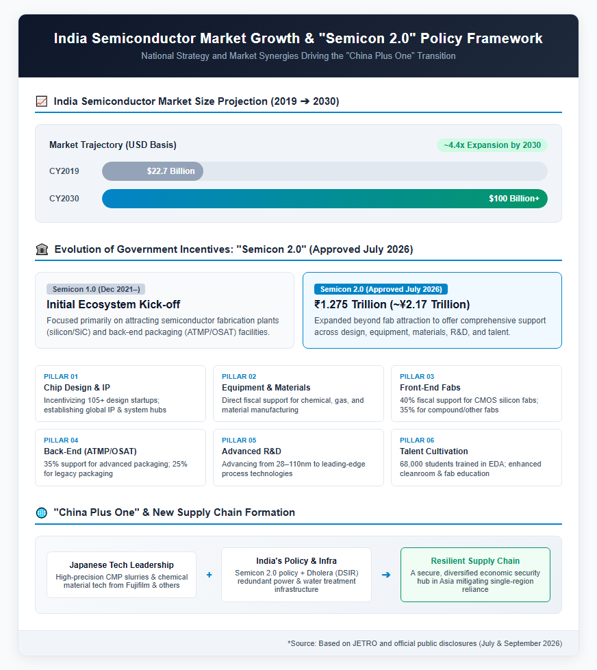
Driven by rapid economic growth and surging demand for electronic devices, India’s semiconductor market is experiencing explosive expansion. The market size, which stood at \$22.7 billion in 2019, is projected to surpass \$100 billion by 2030.
This rapid expansion is underpinned by aggressive industrial policies enacted by the Indian government. In December 2021, the government launched “Semicon 1.0” to kickstart the domestic chip ecosystem, successfully attracting major global semiconductor players. Building on this momentum, the Cabinet approved the second-phase policy, “Semicon 2.0,” in July 2026.
With a budget of 1.275 trillion rupees (approximately 2.1675 trillion yen), Semicon 2.0 moves beyond fab attraction to foster a comprehensive, end-to-end semiconductor ecosystem across six key pillars:
- Semiconductor Design: Incentivizing IP development and supporting semiconductor startups
- Equipment & Materials: Promoting domestic manufacturing of equipment, chemicals, gases, and materials
- Front-End Fab Establishment: Supporting the setup of silicon and compound semiconductor fabs
- Back-End Industry Strengthening: Expanding ATMP (Assembly, Testing, Marking, and Packaging) and OSAT capabilities
- Advanced R&D: Driving next-generation technology research in collaboration with global institutes
- Talent Development: Enhancing specialized education in cleanroom operations and chip design
Fujifilm’s expansion into India aligns perfectly with the localization goals outlined in Semicon 2.0, positioning the company to leverage government financial and infrastructural incentives as it scales operations.
Supply Chain Diversification and the Geopolitical Significance of “China Plus One”
In recent years, prolonged US-China trade tensions, rising geopolitical risks, and pandemic-induced supply chain disruptions have made diversifying away from single-region dependency a top priority for the global semiconductor industry. Amid the “China Plus One” shift, India has emerged as one of the most promising alternative manufacturing destinations worldwide.
Semiconductor fabrication demands a constant, highly stable infrastructure providing power, ultra-pure water, specialty gases, and advanced chemical materials. While infrastructure vulnerabilities and uneven power distribution were historically concerns in India, key focus zones like Dholera in Gujarat feature purpose-built, redundant power substations and dedicated water treatment facilities.
This concentrated infrastructure development significantly mitigates operational risks associated with chip manufacturing. For Fujifilm, establishing a materials base in India extends beyond tapping into a growing domestic market; it represents a strategic move to fortify global semiconductor supply chain security. By combining Japan’s advanced chemical expertise with India’s talent pool and state support, a vital new supply node is taking shape in Asia. Please refer to the following diagram for details.
Fujifilm’s Business Transformation and Future Outlook
Adapting Core Photographic Film Technologies to Advanced AI Semiconductor Materials
Fujifilm’s leadership in the global semiconductor materials sector stems directly from the core chemical and optical technologies it cultivated over decades in photographic film manufacturing. Photographic film is a masterpiece of precision engineering, requiring micro-level, multi-layer coating control, photo-reactive chemistry, and compound dispersion.
These legacy technologies share a profound technical synergy with modern semiconductor fabrication, where extreme miniaturization and 3D stacking are paramount. Fujifilm offers a comprehensive portfolio of advanced process materials, including:
- CMP Slurries: Precision polishing slurries capable of planarizing wafer circuit surfaces with extreme accuracy down to 0.4 nanometers
- ZEMATES: Photosensitive insulating materials utilized for redistribution layers (RDL) and inter-layer insulation
- Wave Control Mosaic: Color filter materials engineered for image sensors in smartphones and advanced cameras
- Post-CMP Cleaners and Ultra-High-Purity Process Chemicals
These specialized materials play an indispensable role in manufacturing cutting-edge GPUs and High Bandwidth Memory (HBM) for generative AI data centers. As a primary profit driver with high operating margins, Fujifilm’s Electronics Materials business is set for further expansion through its entry into the Indian market.
Challenges in Establishing a Local Supply Chain and Key Focus Areas Ahead
While Fujifilm’s entry into India’s semiconductor landscape holds immense promise, establishing seamless local operations presents practical challenges. Semiconductor fabrication requires ultra-high-purity raw materials; thus, Fujifilm must implement rigorous quality management and technical guidance for local Indian chemical suppliers.
Fujifilm aims not merely to operate an isolated plant, but to build an end-to-end domestic supply chain in India—supporting local suppliers to ensure raw material purity and seamless product delivery.
Moving forward, key milestones to watch include:
- The groundbreaking of the Phase 1 plant in October 2026 and infrastructure setup progress
- The timely commencement of commercial production in fiscal year 2027 (ending March 2028)
- Synchronization with the operational timeline of Tata Electronics’ 300mm wafer fab
- Smooth execution of subsidies and regulatory approvals under the Semicon 2.0 framework
As the Japanese and Indian governments deepen cooperation in economic security, Fujifilm’s strategic venture will serve as a crucial bellwether for the successful establishment of India’s semiconductor ecosystem.
Reference Pages
- [FUJIFILM Holdings Press Release] https://holdings.fujifilm.com/ja/news/list/2170
- [Fujifilm Press Release] https://www.fujifilm.com/jp/ja/news/list
【#Fujifilm #SemiconductorMaterials #India #TataElectronics #Semicon2 #SupplyChain #EconomicSecurity】


コメント