Tokyo Electron, a leading semiconductor manufacturing equipment supplier, has announced plans to establish a semiconductor training center in Gujarat, India, in 2027. The initiative aims to address the local shortage of specialized technical talent and build a sustainable industrial foundation within India’s rapidly expanding semiconductor manufacturing ecosystem.
- Key Event Details: Opening a Talent Development Hub in Gujarat State
- Training Program Features and Utilization of DX Technologies
- “Make in India” Policy and the Local Fab Construction Rush
- Strategic Partnerships Between Tokyo Electron and Key Local Enterprises
- An Approach to Resolving the Shortage of Hands-On Manufacturing Engineers
- Future Developments and Key Focus Areas: The Trajectory of Japan-India Co-Creation in Global Supply Chains
Key Event Details: Opening a Talent Development Hub in Gujarat State
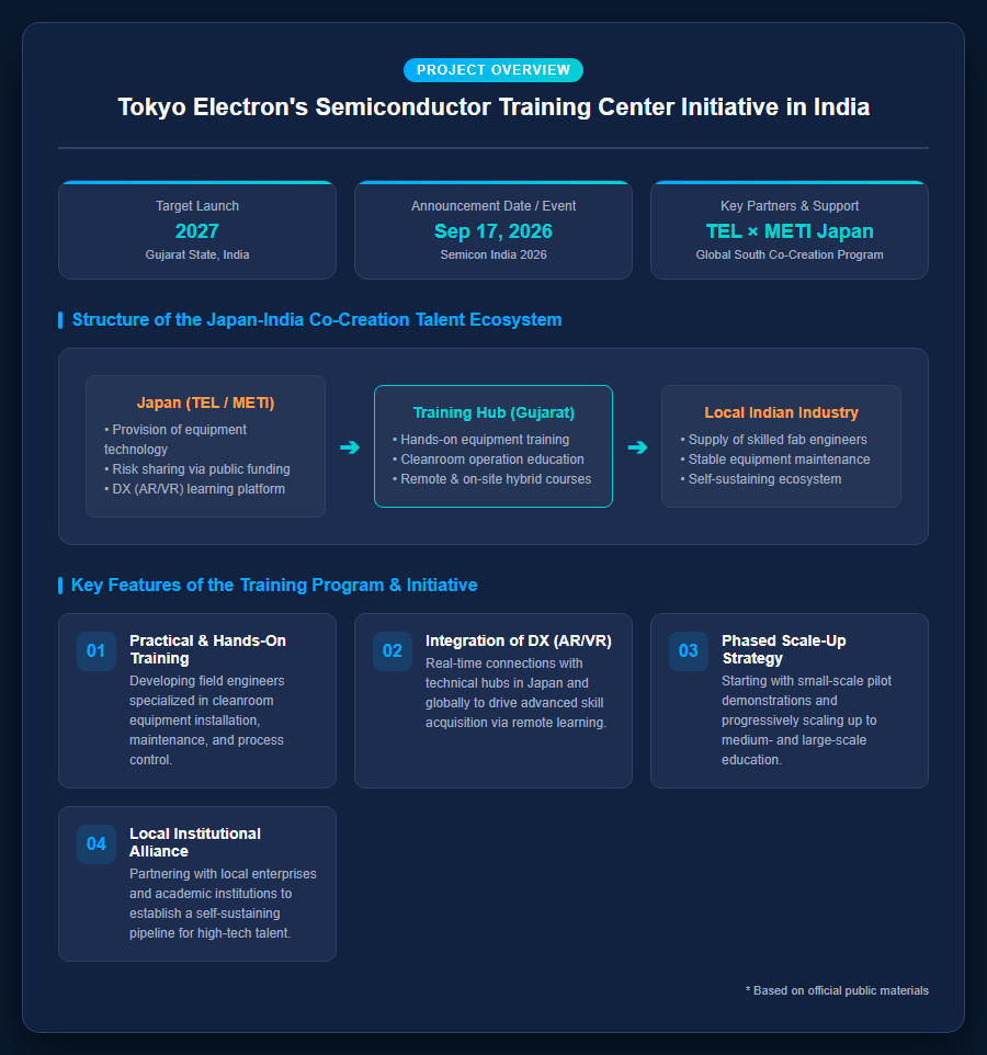
On September 17, 2026, at “Semicon India 2026” in New Delhi, Toshiki Kawai, President and CEO of Tokyo Electron (TEL), revealed plans to establish a semiconductor training center in Gujarat, western India, in 2027. This initiative is being conducted under a strong partnership with the Japanese government, specifically the Ministry of Economy, Trade and Industry (METI).
Driven by the Modi administration’s “Make in India” initiative, the construction of new semiconductor manufacturing fabs by domestic and international companies is accelerating across India. However, securing highly skilled engineers capable of managing cutting-edge semiconductor manufacturing processes, equipment operation, maintenance, and process control remains a major challenge. The training center established by Tokyo Electron focuses specifically on cultivating future fab engineers and equipment engineers, aiming to build a robust local talent pipeline.
This project is being executed as part of a demonstration initiative selected for METI’s FY2024 supplementary budget under the “Global South Future-Oriented Co-Creation Grant Program.” Rather than relying solely on temporary technology transfers, a key defining feature is its direct collaboration with local Indian companies and educational institutions to build a self-sustaining ecosystem that continuously produces high-tech engineers.
Please refer to the following diagram.
Training Program Features and Utilization of DX Technologies
The training center in Gujarat will offer a hybrid educational program combining hands-on training using actual equipment with theoretical instruction. Centered on developing field engineers responsible for installing, maintaining, and inspecting semiconductor manufacturing equipment, the program systematically teaches operation and maintenance techniques required inside strictly controlled cleanroom environments.
In addition, the active integration of Digital Transformation (DX) technologies is a major highlight of this initiative. Specifically, by building a remote education system leveraging Augmented Reality (AR) and Virtual Reality (VR), the center will connect local Indian facilities with technical hubs in Japan and around the world in real time. This creates an intuitive learning environment where trainees can master complex internal equipment structures and advanced troubleshooting procedures on-site.
The project adopts a phased deployment approach, starting with small-scale educational demonstrations, expanding to medium-scale training, and ultimately scaling into a large-scale talent development system. By utilizing public support to mitigate initial investment risks while accelerating demonstration and expansion, Tokyo Electron aims to strengthen its service capabilities and further expand its market share in the Indian semiconductor market.
Background of Building a Semiconductor Ecosystem in the Indian Market
“Make in India” Policy and the Local Fab Construction Rush
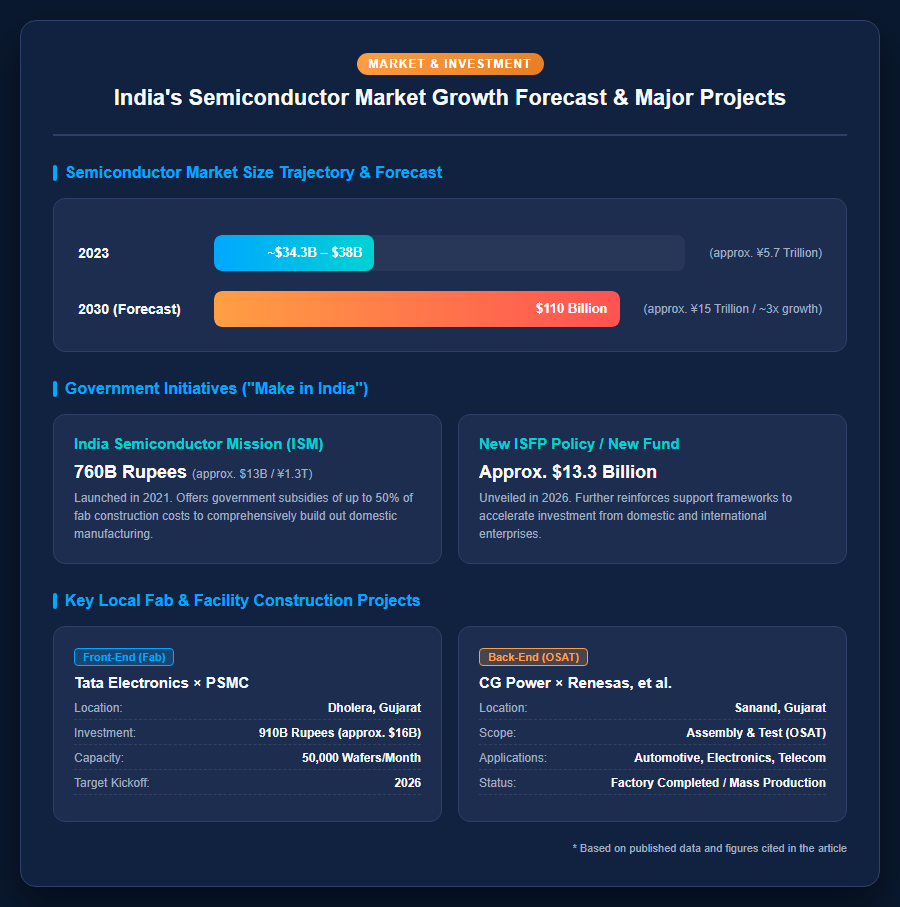
The Indian government is aggressively pushing for domestic semiconductor production under its “Make in India” banner to upgrade national industries and mitigate security risks. In 2021, it launched the India Semiconductor Mission (ISM) with a budget of 760 billion rupees (approx. \$13 billion), offering generous incentives including government subsidies of up to 50% of fab construction costs. In 2026, the government further reinforced its support framework by introducing a new fund worth approximately \$13.3 billion alongside the new “ISFP” policy.
Backed by this policy momentum, major conglomerates and global enterprises are racing to build facilities across India. In Dholera, Gujarat, Tata Electronics—a subsidiary of the Tata Group—in partnership with Taiwan’s PSMC, is constructing a front-end fab with an investment of 910 billion rupees (approx. \$16 billion) and a targeted monthly capacity of 50,000 wafers, aiming for operational kickoff in 2026. Meanwhile, in Sanand, Gujarat, CG Power is advancing the construction of an outsourced semiconductor assembly and test (OSAT) facility in collaboration with Renesas Electronics and other partners.
India’s semiconductor market size is projected to surge from approximately \$34.3 billion to \$38 billion (approx. 5.7 trillion yen) in 2023 to \$110 billion (approx. 15 trillion yen) by 2030, propelled by explosive demand for smartphones, automotive electronics, and AI applications.
Please refer to the following diagram.
Strategic Partnerships Between Tokyo Electron and Key Local Enterprises
With the surge in new semiconductor factory construction, the demand for local support from equipment manufacturers has surged dramatically. In September 2024, Tokyo Electron announced a comprehensive business alliance with Tata Electronics. Under this partnership, TEL supplies cutting-edge semiconductor manufacturing equipment and provides technical training and R&D support for Tata’s front-end fab in Gujarat as well as its back-end packaging facility under construction in Jagiroad, Assam.
Tokyo Electron holds a dominant global market share of approximately 90% in coater/developers, and nearly 100% for Extreme Ultraviolet (EUV) lithography systems. Boasting a broad lineup spanning front-end process tools to back-end packaging technologies—such as etch and deposition equipment—TEL is indispensable to establishing semiconductor production lines.
Furthermore, beyond establishing marketing bases, TEL is advancing plans to open a new development center in Bengaluru, southern India, in the summer of 2025, dedicated to equipment design and software development. The company plans to scale the center to 300 personnel by 2027, primarily hiring local talent. Together with the establishment of the new training center, Tokyo Electron is solidly establishing a foundation for both technological development and talent operations within India.
Significance for Japanese Companies and Future Outlook
An Approach to Resolving the Shortage of Hands-On Manufacturing Engineers
India produces a massive number of Science, Technology, Engineering, and Mathematics (STEM) graduates every year, earning global recognition as a powerhouse of advanced IT talent and software designers. Leading U.S. chipmakers such as AMD, Intel, and Qualcomm have established major design centers in India to leverage this technical expertise.
However, operating actual semiconductor manufacturing lines requires hands-on engineers who can accurately operate, maintain, and optimize complex equipment based on specialized knowledge in chemistry, physics, materials science, and mechanical control. Currently, India’s talent pool is heavily skewed toward circuit design, leaving a critical shortage of field engineers needed to sustain volume manufacturing fabs.
The talent development ecosystem led by Tokyo Electron offers a direct approach to rectifying this imbalance. By transferring Japan’s long-cultivated manufacturing know-how and advanced equipment operation techniques to local personnel, TEL will help build the foundation necessary to improve yields and ensure stable operations in India’s semiconductor fabs.
Future Developments and Key Focus Areas: The Trajectory of Japan-India Co-Creation in Global Supply Chains
Against the backdrop of prolonged U.S.-China tensions and rising geopolitical risks, global semiconductor supply chains are undergoing significant restructuring. For equipment suppliers that previously depended heavily on the Chinese market, expanding into emerging markets like India has become a top strategic objective.
Significant hurdles remain before India’s semiconductor industry becomes fully operational, including infrastructure challenges such as securing reliable supplies of power, water, and industrial gases, as well as establishing local supply chains for raw materials like silicon wafers. Nevertheless, the growth potential backed by massive domestic demand and strong government leadership is immense.
Tokyo Electron’s establishment of the training center and talent ecosystem will not only help the company secure a de facto standard in the local market, but also serve as a crucial stepping stone for Japanese industry as a whole to participate in India’s growth from legacy nodes to leading-edge processes. As Japan, with its strength in manufacturing, and India, with its strength in design and human resources, deepen their complementary relationship, industry observers are closely watching whether this partnership will forge a new cornerstone in next-generation global semiconductor supply chains.
References
-
[Tokyo Electron News Release (Global South Future-Oriented Co-Creation Grant Program)] https://www.tel.co.jp/news/topics/2026/20260424_001.html
-
[Tokyo Electron News Release (Business Alliance with TATA Electronics)] https://www.tel.co.jp/news/topics/2024/20240910_001.html
[#TokyoElectron #India #Semiconductor #TalentDevelopment #Gujarat #METI #MakeInIndia]

コメント