On September 29, 2026, Hamamatsu Photonics K.K. announced and began accepting orders for the “iPHEMOS-DDX,” an inverted emission microscope compatible with advanced semiconductor packages such as AI chiplets and high-bandwidth memory (HBM). This release comes against the backdrop of increasingly three-dimensional and larger semiconductor structures driven by the rapid expansion of generative AI, along with a sharp surge in demand for failure analysis to improve manufacturing yields.
- Surge in Failure Analysis Needs Due to Higher AI Chip Integration and Key Points of New Equipment
- Optimization of the Analysis Environment via a Three-Way Direct Docking Structure
- A multi-platform integrating luminescence, thermal, and laser analysis into a single unit
- High-Precision Defect Identification Mechanisms in 2.5D/3D Packages and HBM
- The Market Trend of Shifting from Sampling to 100% Automated Inspection and the Role of the New Factory in South Korea
- Future Outlook and Key Focus Areas for the Evolution of the Advanced Packaging Market
Surge in Failure Analysis Needs Due to Higher AI Chip Integration and Key Points of New Equipment
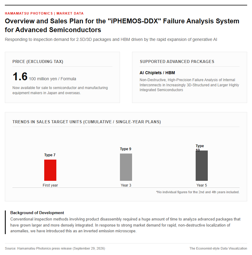
On September 29, 2026, Hamamatsu Photonics K.K. began taking orders for the “iPHEMOS-DDX,” an inverted emission microscope designed for electrical fault analysis (EFA) of advanced semiconductor packages. The base unit is priced at 160 million yen (excluding tax) and will be sold to semiconductor manufacturers and manufacturing equipment makers both in Japan and overseas. The company has set sales targets of 7 units in the first year, 9 units in the third year, and 10 units in the fifth year.
Behind this is the increasing structural complexity of AI chips, driven by the rapid evolution of generative AI. In current state-of-the-art AI processors, the adoption of 2.5D packages—where High Bandwidth Memory (HBM) is placed around a central logic IC—and 3D packages (AI chiplets), which stack chips vertically, has become mainstream. These advanced packages have grown larger due to high-density integration, making it extremely difficult to pinpoint minute defects occurring in internal wiring and joints. Because conventional methods of dismantling and inspecting products take an enormous amount of time, there has been a strong demand for advanced analysis equipment capable of non-destructively and accurately identifying anomaly locations. As shown in the conceptual diagram below, the importance of inspection in the manufacturing process is increasing.
Optimization of the Analysis Environment via a Three-Way Direct Docking Structure
One of the major features of “iPHEMOS-DDX” is its flexible mechanical structure that supports direct tester docking from three directions. For cutting-edge devices such as AI chiplets, electrical failure analysis (EFA) is performed while they are connected to a semiconductor tester and operated at a high clock frequency of 1 GHz or more, in order to capture abnormal phenomena that occur during actual operation.
Conventional devices had limitations on the connection direction with the tester, posing significant constraints on installation within customer lab layouts and existing measurement environments. By enabling direct docking from three directions, this device allows for smooth integration into existing inspection lab environments. As a result, the following benefits are achieved.
- Building Flexible Layouts for Analysis Environments Centered Around Testers
- Significant reduction in setup man-hours by simplifying the connection jig
- Stable anomaly detection in high-speed signal transmission environments close to actual operating conditions
Additionally, it features a low-temperature and highly stable design, enabling stable measurements with thermal drift minimized to the absolute minimum even during extended observations. The actual device is also scheduled to be showcased at the international conference “ISTFA 2026,” to be held in Texas, USA, from October 4 to 8, and it is expected to contribute to reforming laboratory environments for semiconductor manufacturers worldwide.
Integration of Seven Analysis Methods and the Latest Advanced Package Analysis Technologies
A multi-platform integrating luminescence, thermal, and laser analysis into a single unit
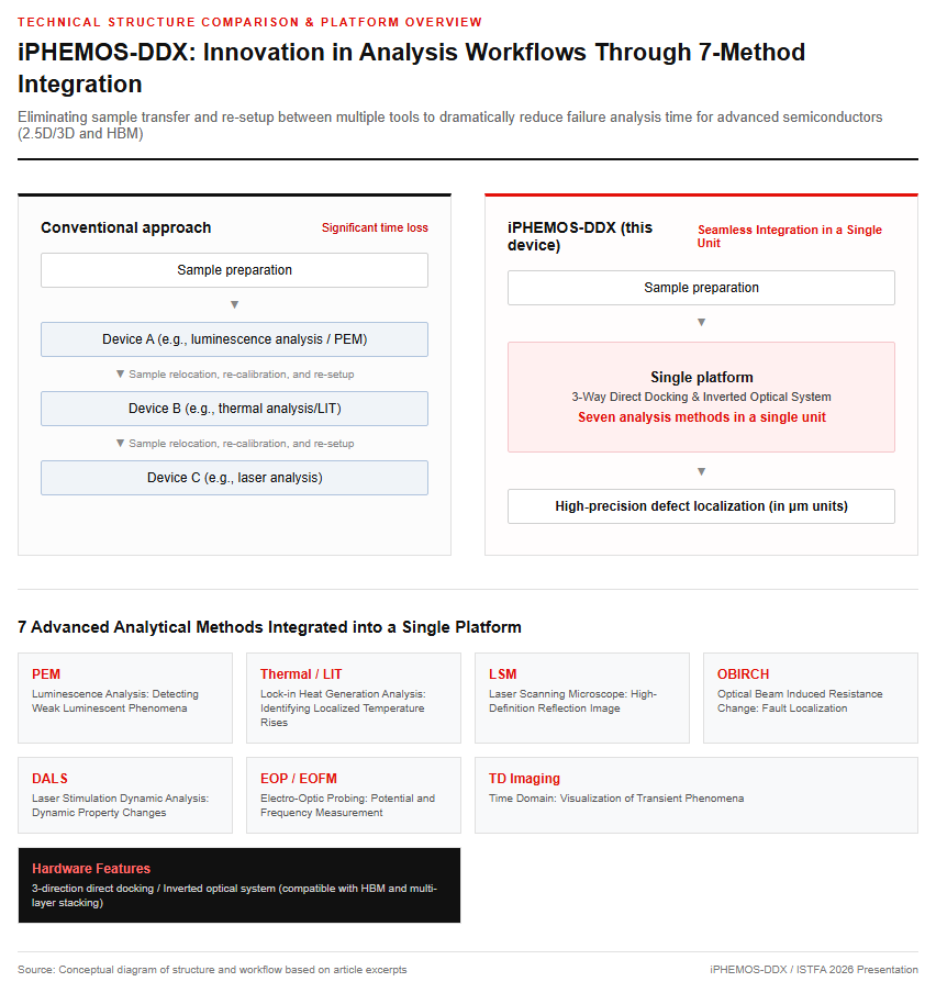
In conventional semiconductor failure analysis, it has been common to use different measurement equipment depending on the phenomenon and nature of the defect. However, moving the samples for each analysis method and performing re-setup and recalibration has been a major time loss throughout the entire analysis workflow.
“iPHEMOS-DDX” integrates the following seven advanced analysis methods on a single platform.
- PEM (Photoemission Microscopy): Detects faint light emission phenomena associated with current leakage, etc.
- Thermal/LIT (Lock-In Thermography): Non-destructively and with high sensitivity, identifying localized temperature rises
- LSM (Laser Scanning Microscope): Acquires high-definition reflection images of surface and internal structures
- OBIRCH (Optical Beam Induced Resistance Change): Identifying defect locations from changes in wiring resistance caused by laser irradiation
- DALS (Laser Stimulation Dynamic Analysis): Analyzing changes in dynamic operating characteristics
- EOP/EOFM (Electro-Optical Probing / Frequency Mapping): Optically measures potential changes and operating frequencies during operation.
- TD Imaging (Time-Domain Imaging): Visualization of Transient Phenomena Along the Time Axis
By seamlessly combining not only luminescence analysis, but also thermal analysis and laser analysis into a single system, it eliminates errors associated with sample movement and setup time, thereby dramatically reducing failure analysis time.
High-Precision Defect Identification Mechanisms in 2.5D/3D Packages and HBM
In 2.5D and 3D packages, multiple heterogeneous chips are connected at high density via silicon interposers and TSVs (through-silicon vias). Particularly in HBM (High Bandwidth Memory), which is essential for generative AI GPUs, a large number of thinned DRAM dies are vertically stacked, making it extremely difficult to identify at which layer and at which bonding point a short circuit or disconnection has occurred.
By adopting an inverted optical system, this device facilitates observation from the backside of the package and captures sources of minute light emission and heat generation with high precision. By inputting high-speed test patterns from a tester and combining seven analysis methods, it identifies the locations of physical defects lurking deep inside complex stacked structures with micrometer-level precision. As shown in the analysis image below, minute defects between heterogeneous chips can also be clearly visualized.
This high-precision defect identification mechanism enables semiconductor designers and process development engineers to rapidly approach the root cause of defects. It significantly shortens the yield improvement period during the ramp-up phase of new processes, serving as a technical foundation that supports the early market introduction of cutting-edge AI chips.
Market Expansion, Ripple Effects on the Semiconductor Industry, and Future Outlook
The Market Trend of Shifting from Sampling to 100% Automated Inspection and the Role of the New Factory in South Korea
In the semiconductor industry, a major qualitative shift is currently taking place in how inspection processes are conducted. Conventionally, in the manufacturing of HBM and high-priced logic ICs, “sampling inspection” (sampling a certain percentage of items for testing) has been the mainstream approach. However, because cutting-edge AI chips are extremely costly to manufacture and a single defect leads to the scrapping of an entire package, there is a rapid transition toward “100% automated inspection” to improve yields and ensure quality.
To meet this growing demand, Hamamatsu Photonics is actively strengthening its overseas manufacturing bases. The company’s South Korean subsidiary, HAMAMATSU PHOTONICS KOREA, newly established the Dongtan plant in Hwaseong, Gyeonggi Province, and commenced full-scale operations in March 2025.
- Location: Hwaseong-si, Gyeonggi-do, South Korea (Total floor area: 2,617 square meters)
- Total construction cost: Approx. 400 million yen
- Production capacity: Approximately 11 billion yen in terms of annual sales (approx. 100 billion won)
South Korea is a strategic hub where the world’s leading memory semiconductor manufacturers are concentrated, and this new plant serves as a base for enhancing the manufacturing capacity of failure analysis equipment and developing automation features (such as automatic viewpoint switching and high-speed whole-wafer inspection). The establishment of a supply system through the new plant is strongly boosting the global expansion of “iPHEMOS-DDX”.
Future Outlook and Key Focus Areas for the Evolution of the Advanced Packaging Market
The biggest point of focus moving forward is the expanding role of analysis equipment accompanying the further advancement of semiconductor packaging technology. Beyond the growth of the generative AI market, the practical application of next-generation computing infrastructure—such as optical-electrical fusion technology combining light and power (like the IOWN initiative) and quantum computers—is expected to advance. In these cutting-edge fields, in addition to conventional electrical signal measurement, the analysis accuracy of optical signals and minute thermal control will be the key to determining the success or failure of commercialization.
Hamamatsu Photonics’ newly introduced “iPHEMOS-DDX” aims to secure its position as the golden standard in cutting-edge 2.5D/3D package analysis. Rather than stopping at mere failure analysis, it serves as part of an ecosystem that feeds collected data back into the manufacturing process, promoting yield improvement and automation across the entire line.
Even amidst changing international technology frictions and export control policies, the company’s technological superiority in optical metrology and non-destructive testing remains highly evaluated. Key observation points in the future market will be whether they can achieve their annual sales target of 10 units in the fifth year, and whether they can become established as a 100% inspection and 100% analysis platform on the mass production lines of major AI chip manufacturers.
Reference Page
- [Hamamatsu Photonics Press Release] https://prtimes.jp/main/html/rd/p/000000069.000081184.html
- [Hamamatsu Photonics Product Information] https://www.hamamatsu.com/jp/ja/product/semiconductor-manufacturing-support-systems/failure-analysis-system/C18040-11.html
- 【Hamamatsu Photonics Official Website】https://www.hamamatsu.com/jp/ja.html
【#HamamatsuPhotonics #SemiconductorFailureAnalysis #iPHEMOS_DDX #AIChip #HBM #AdvancedPackaging #EmissionMicroscope】


コメント