Rapidus, aiming for the domestic production of next-generation semiconductors, has strengthened its collaboration in the field of advanced semiconductor design with 17 companies and organizations, including Toshiba and other major domestic corporations and research institutions. Ahead of the planned mass production of cutting-edge 2nm (nanometer) generation logic semiconductors in 2027, this comes as building a design ecosystem and securing design talent—beyond merely preparing production lines—have become top priorities.
- Key takeaway of the event: Advanced design collaboration between Rapidus, Toshiba, and 17 other companies
- Overcoming Design Walls and Bottlenecks in the 2nm Generation
- Lessons from the Past and the Transition to a “Design-Led” Ecosystem
- Cumulative Government Support Totaling 3 Trillion Yen and the Integration of SATAS (LSTC)
- Confrontation with TSMC and the Latest Trends in the Global 2nm Competition
- Future Outlook and Key Focus Areas: Roadmap to Mass Production and Customer Acquisition
Key takeaway of the event: Advanced design collaboration between Rapidus, Toshiba, and 17 other companies
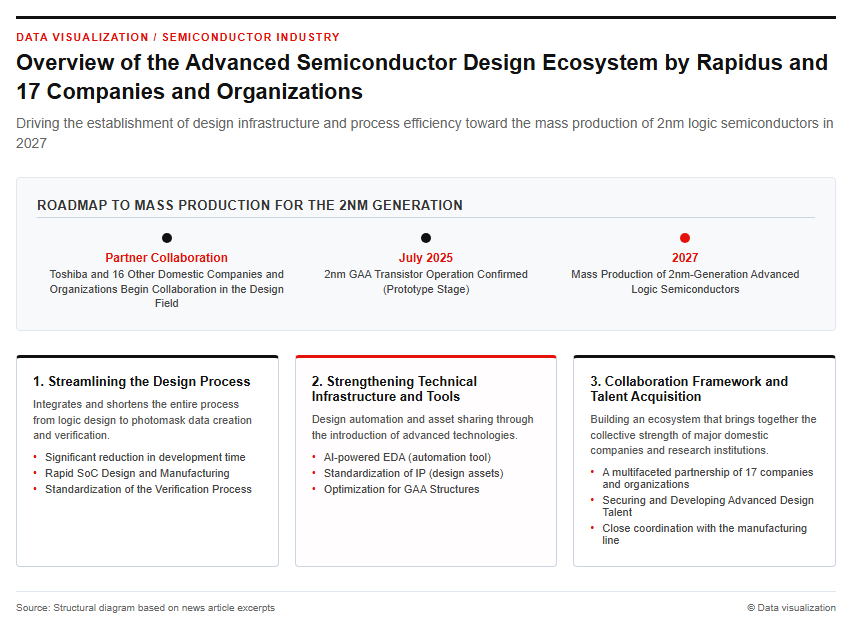
Rapidus has launched a collaborative framework for cutting-edge 2nm-generation semiconductor design, partnering with 17 companies and organizations, including major Japanese semiconductor and electronics manufacturers such as Toshiba and technology research associations. Through this partnership, the companies aim to establish solutions that streamline the entire design process—from logic design to photomask data creation and verification—significantly shortening development times. Specifically, efforts will be made to introduce AI-driven electronic design automation (EDA) tools and standardize IP (intellectual property). In July 2025, Rapidus successfully verified the operation of its 2nm GAA (gate-all-around) transistors, shifting its focus from the prototyping stage to mass production. However, in the semiconductor business, rapidly designing and manufacturing advanced SoCs (system-on-a-chip) tailored to customer demands requires not only in-house manufacturing capabilities, but also a strong collaborative foundation with diverse design partners. The figure below illustrates the overall picture of the design ecosystem formed by this 17-company collaboration.
By combining the design know-how for power semiconductors and system LSIs that Toshiba has cultivated over many years with Rapidus’s cutting-edge manufacturing processes, Toshiba aims to secure orders in high-value-added fields such as autonomous driving and AI data centers.
Overcoming Design Walls and Bottlenecks in the 2nm Generation
In the development of cutting-edge 2nm process semiconductors, “the shortage of design talent” and “the complexity of the design process” are emerging as the biggest bottlenecks. As the circuit line width enters the 2nm generation, it is necessary to highly integrate tens of billions of transistors, creating a risk that traditional design methods will prolong the development turnaround time (TAT). TSMC, the global foundry king, dominates the market by building an ecosystem with over 30 specialized design houses and EDA vendors. For Rapidus as well, abandoning self-reliance and building an open collaboration network with external companies was an urgent task. Surveys as of 2026 also point out that the supply of domestic advanced semiconductor design engineers falls significantly short of demand. In this partnership, design automation through the use of cutting-edge tools will be promoted, including the integration of Cadence’s agent-based AI design solutions and AI chip design cooperation with Tenstorrent. As a result, an environment will be established where even customer companies that can only perform logic design can smoothly develop and ship chips for Rapidus’s 2nm line.
Industrial Structure Transformation and the Role of Government and Public-Private Support
Lessons from the Past and the Transition to a “Design-Led” Ecosystem
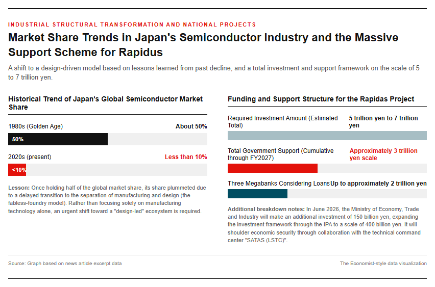
Looking back at the history of Japan’s semiconductor industry, it once accounted for roughly 50% of the global market share in the 1980s, but was slow to adapt to the subsequent separation of design and manufacturing (the fabless-foundry model), leading to a decline to less than 10% by the 2020s. Elpida Memory, which collapsed in 2012, boasted world-class microfabrication technology, yet struggled with financial strategy and the establishment of customer-engagement frameworks. Meanwhile, Renesas Electronics has staged a comeback following structural reforms. The biggest lesson learned from the past defeat of Japan’s “Hinomaru semiconductors” is the hard truth that “manufacturing technology alone cannot win in the market.” In today’s semiconductor market—exemplified by companies like NVIDIA—those with superior design capabilities and software infrastructure (such as CUDA) command the market’s added value and pricing power. For Rapidus to succeed as a contract foundry, it must not merely process wafers; it needs to build a flexible framework capable of addressing customer demands from the design stage onward, working alongside key domestic players such as Toshiba. Shifting from a manufacturing-centric mindset to a “design-driven” industrial ecosystem will be the key to determining the success or failure of Japan’s semiconductor resurgence.
Cumulative Government Support Totaling 3 Trillion Yen and the Integration of SATAS (LSTC)
The Rapidus project is positioned not merely as the business of a single company, but as a national economic security strategy. The Ministry of Economy, Trade and Industry (METI) is expanding the investment framework through the Information-processing Promotion Agency (IPA) to a scale of 400 billion yen—including an additional investment of 150 billion yen in June 2026—and total government support through fiscal 2027 is expected to reach a cumulative scale of approximately 3 trillion yen. Furthermore, alongside considerations by three megabanks, including MUFG Bank, for loans of up to 2 trillion yen, efforts are underway to secure the necessary investment amount, estimated to be between 5 trillion and 7 trillion yen in total. The technological command center supporting this colossal support is the Leading-edge Semiconductor Technology Center (LSTC), commonly known as “SATAS.” The structural diagram below illustrates the division of roles between the research institution SATAS and Rapidus, which is responsible for manufacturing.
SATAS serves as the “brain” connecting the National Institute of Advanced Industrial Science and Technology (AIST), universities, and overseas research institutions, taking charge of research into next-generation process technologies of 2nm and beyond and the development of design infrastructure. Rapidus as the “muscle” and SATAS as the “brain” will unite, and it is expected to play a role as a “connecting device” that swiftly translates research outcomes into commercialization through collaboration with 17 companies, including Toshiba.
Positioning in the Global Market and Future Outlook
Confrontation with TSMC and the Latest Trends in the Global 2nm Competition
In the global advanced semiconductor market, Taiwan’s TSMC holds a market share of approximately 72%, reigning as the absolute king. TSMC is set to begin mass production of its 2nm process (N2) in the second half of 2025, positioning itself to monopolize orders from major customers such as Apple and NVIDIA. Meanwhile, South Korea’s Samsung Electronics and U.S.-based Intel are continuing to make massive investments toward the mass production of the 2nm and 1.8nm generations. Against such giant competitors, it is no easy feat for latecomer Rapidus to achieve a breakthrough head-on using the same mass-production model. Consequently, Rapidus has adopted a differentiation strategy centered on high-mix, low-volume production and fast delivery times (reduced turnaround times) as its core strengths. Its policy is to capture demand for custom chips optimized for individual customers across areas such as automotive, AI inference, and industrial equipment. However, high-mix, low-volume production entails frequent switching of manufacturing processes, making the maintenance of factory utilization rates and cost management extremely difficult. Through collaboration with 17 companies and organizations—including Toshiba—partnered with this time, standardizing high-quality, application-specific IP and design verification mechanisms in advance will be an essential prerequisite to delivering short-lead-time services that justify their high unit prices.
Future Outlook and Key Focus Areas: Roadmap to Mass Production and Customer Acquisition
The biggest focus moving forward is the steady execution of the roadmap toward the full-scale mass production of 2nm semiconductors scheduled for fiscal 2027, and the acquisition of anchor customers (key clients) on a mass-production scale. Rapidus is proceeding with the operation of a prototype line at its factory in Chitose City, Hokkaido (IIM-1), and improving yields and stabilizing the manufacturing process are top priorities. Because semiconductor fabs are structured to incur losses due to massive fixed costs if they cannot maintain high operating rates, how many firm orders can be secured by the start of mass production will dictate the viability of the business. Furthermore, establishing a supply chain not only for front-end processes (circuit formation) but also for back-end processes (packaging) such as chiplet technology and 2.5D/3D integration is an urgent necessity. Key indicators that investors and business professionals should watch moving forward include the budget execution status of government support, loan terms from private financial institutions, and the disclosure of specific mass-production contracts with major domestic and overseas AI and automotive manufacturers. Whether the collaborative achievements with 17 domestic companies, including Toshiba, will materialize into actual product development and mass-production orders will serve as a true litmus test for the revival of Japan’s semiconductor industry.
Reference Page
- [Rapidus Inc. Official Announcement] https://www.rapidus.inc/news_topics/
- [Ministry of Economy, Trade and Industry: Next-Generation Semiconductors and Related Information] https://www.meti.go.jp/
【#Rapidus #Semiconductor #Toshiba #2nm #METI #SATAS #SemiconductorDesign #JapaneseEconomy】

コメント