Hitachi High-Tech and Germany’s ZEISS have strengthened their joint development framework for next-generation multi-beam electron beam inspection systems. The background includes the increasing difficulty of detecting sub-10nm micro-defects associated with the introduction of 2nm nodes and High-NA EUV, as well as a sharp increase in the demand for high-speed inspection on mass production lines.
- Joint Announcement of Next-Generation Multi-Beam Electron Beam Inspection System by Hitachi High-Tech and German ZEISS
- Limitations of Existing Inspection Technologies Associated with Semiconductor Scaling and the Introduction of High-NA EUV
- Higher sensitivity through 91-beam multi-beam technology and speeds tens of times faster than a single beam
- Addressing Sub-10nm Micro-Defects, In-Film Defects, and Voltage Contrast Inspection
- AI-Powered Inspection Algorithm and Digitized Asset Integration via HMAX Industry
- Accelerating Customer Co-Creation and Evaluation Validation to Secure POR in the Field
- Outlook and Future Key Focus Areas for the Next-Generation Process Control Market
Joint Announcement of Next-Generation Multi-Beam Electron Beam Inspection System by Hitachi High-Tech and German ZEISS
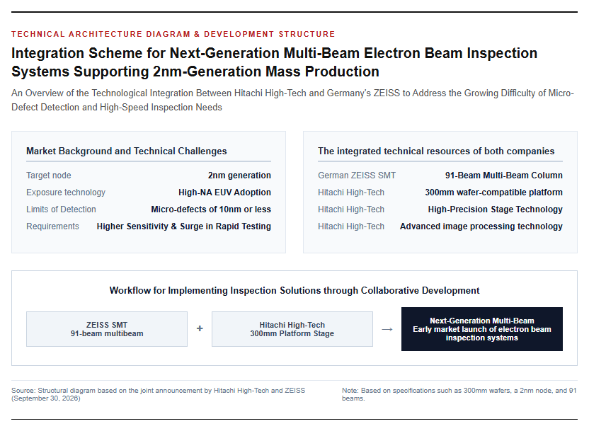
On September 30, 2026, Hitachi High-Tech Corporation announced that it will strengthen its development framework for the next-generation multi-beam electron beam inspection system that it has been jointly developing with Germany’s ZEISS Semiconductor Manufacturing Technology (ZEISS SMT). The two companies have been advancing the development of a high-sensitivity and high-speed inspection system by integrating Hitachi High-Tech’s long-cultivated 300mm wafer-compatible inline metrology and inspection system platforms, high-precision stage technology, and image processing technology with ZEISS SMT’s renowned 91-beam multi-beam column technology.
This structural enhancement responds to the rapidly growing demand for inspection performance in the mass-production sites of advanced logic semiconductors and memory devices. In the global market, semiconductor device manufacturing is undergoing a historical turning point with the introduction of the 2nm node and High-NA EUV. As circuit patterns become ultra-minaturized, yield management on manufacturing lines has become a critical factor that dictates profitability. By accelerating the pace of joint development, both companies aim to rapidly introduce innovative inspection solutions capable of detecting micro-defects with high sensitivity and high speed to mass-production environments. Please refer to the figure below.
Limitations of Existing Inspection Technologies Associated with Semiconductor Scaling and the Introduction of High-NA EUV
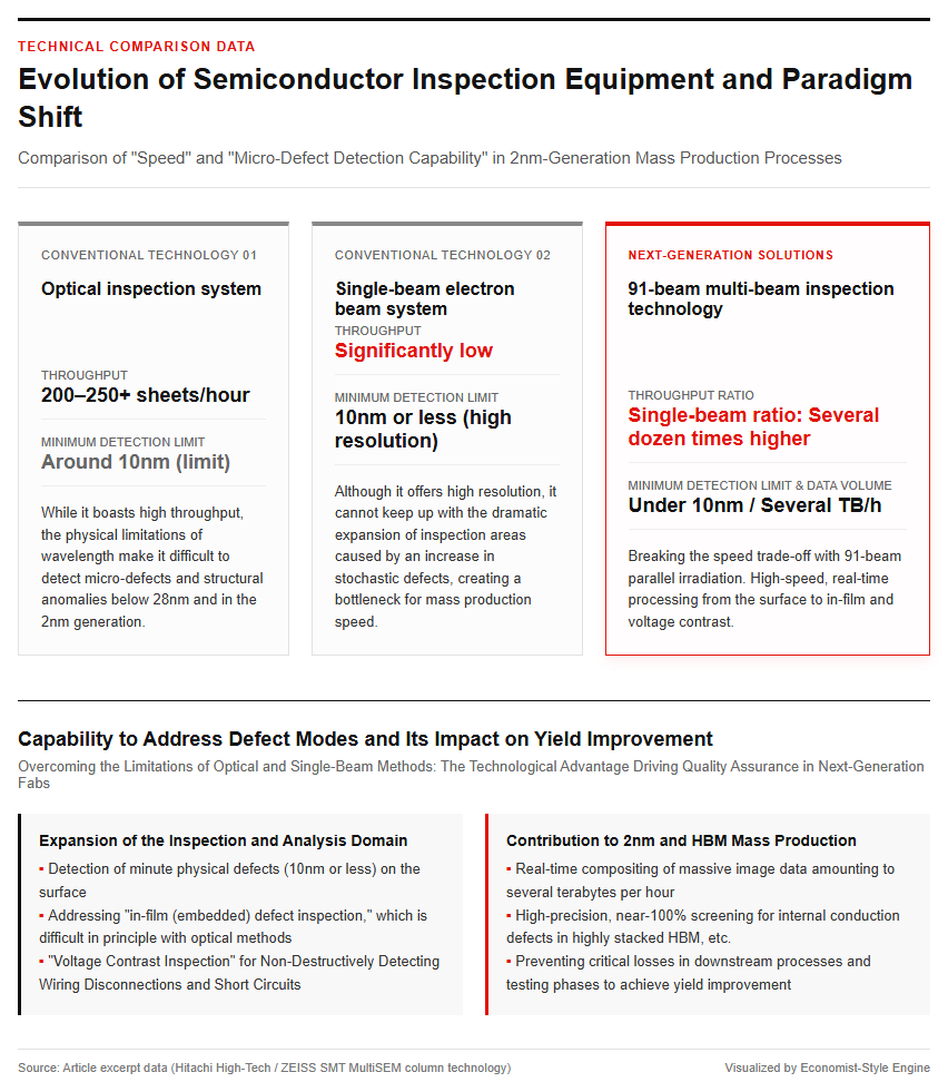
In cutting-edge semiconductor manufacturing plants, optical inspection systems and single-beam electron-beam inspection systems have traditionally been used selectively for wafer inspection after circuit pattern formation depending on the application. Optical inspection systems boast high throughput capable of processing 200 to over 250 wafers per hour, but due to the physical limitations of wavelength, it has become difficult to stably detect micro-defects of around 10 nm. From 2025 onward, as process nodes of 28 nm and below become operational in many advanced fabs and the transition to the 2 nm generation further progresses, structural anomalies that cannot be caught by optical inspection have become a serious challenge.
On the other hand, single-beam electron beam inspection systems, which use a single electron beam, have high resolution and have been utilized inline for specific hotspot inspections and other applications. However, with the three-dimensional and increasingly complex device structures, stochastic defects caused by exposure variations in the EUV lithography process are increasing. As a result, the areas to be inspected (care areas) and the number of inspection layers have increased dramatically, exposing the limitation that the single-beam method suffers a significant drop in throughput and cannot keep up with the speed of mass production lines.
Higher sensitivity through 91-beam multi-beam technology and speeds tens of times faster than a single beam
Multi-beam electron beam inspection technology is positioned as the sole solution to overcome the speed-and-sensitivity trade-off facing existing technologies. ZEISS SMT’s MultiSEM column technology irradiates 91 electron beams for parallel scanning, dramatically increasing the parallelism of irradiation and image acquisition compared to conventional single-beam systems. By integrating a highly sensitive detector and a parallel data processing system that correspond to this, it becomes possible to visualize ultra-fine regions in an extremely short time.
In the development equipment being advanced by Hitachi High-Tech and ZEISS SMT, on-site evaluations at customer factories using prototype units have already begun. This verification experiment demonstrated that the equipment can capture microscopic defects of 10 nm or less—which were difficult to detect with conventional optical inspection systems—while performing inspection processing at dozens of times the speed of conventional single-beam electron beam inspection systems. The achievement of synthesizing massive amounts of image data reaching several terabytes per hour in real-time and realizing high-speed scanning while maintaining a high defect detection rate represents a major technological breakthrough for the 2nm-generation mass production process.
Technical features and approach to yield improvement
Addressing Sub-10nm Micro-Defects, In-Film Defects, and Voltage Contrast Inspection
The newly announced multi-beam electron beam inspection technology goes beyond the detection of microscopic physical defects exposed on the surface, offering advanced analytical capabilities for a diverse range of failure modes. It truly demonstrates its value particularly in “in-film (buried) defect inspection” and “Voltage Contrast inspection,” which are fundamentally difficult for optical inspection systems to handle. Voltage contrast inspection is a technique that detects wiring breaks and short circuits within the internal structures of multilayer interconnects and through-silicon vias (TSVs) through differences in contrast images caused by potential differences, enabling in-line, non-destructive evaluation without destroying the electrical characteristics of the device.
In the manufacturing of cutting-edge logic chips of 2nm and below, as well as highly stacked HBM (High Bandwidth Memory), the economic loss resulting from defects discovered in post-processing or final testing stages is exceptionally large. Screening for microscopic voids and conduction failures within the film halfway through the stacked structure with near 100% accuracy is an absolute requirement for improving yields and reducing manufacturing costs. This multi-beam system has the capability to simultaneously and rapidly flush out physical defects of 10nm or less and electrical anomalies, playing a role in significantly enhancing the reliability of quality assurance in state-of-the-art fabs. Please refer to the figure below.
AI-Powered Inspection Algorithm and Digitized Asset Integration via HMAX Industry
In addition to hardware evolution of the equipment, approaches in terms of software and data utilization are also being strengthened. In this strengthening of the joint development framework, the resources of both companies are being combined to promote the integration of “AI-enabled inspection algorithms.” By using machine learning and self-supervised learning to automatically and accurately classify true defects and pseudo-defects from the massive amount of noise and background patterns generated by high-resolution multi-beam images, the false detection rate is reduced and the speed of inspection judgment is improved.
Furthermore, Hitachi High-Tech offers the “HMAX Industry for Semiconductors” solution, which combines advanced AI with data and domain knowledge obtained from the company’s extensive installation track record (digitalized assets) of critical dimension SEMs and measurement/inspection systems. By analyzing defect data collected in real-time from multi-beam inspection systems and providing immediate feedback to preceding and subsequent manufacturing processes such as exposure and etching, it achieves optimization of manufacturing conditions and predictive maintenance for anomaly prevention. Through the integration of hardware, AI software, and digital infrastructure, it helps significantly shorten the Time to Market for products.
Future Mass Production Adoption and Impact on the Advanced Semiconductor Market
Accelerating Customer Co-Creation and Evaluation Validation to Secure POR in the Field
For next-generation inspection equipment to be actually integrated into mass-production lines, acquiring certification for POR (Process of Record)—the manufacturing process standard of device manufacturers—is essential. Hitachi High-Tech is leveraging its customer network built with major global semiconductor manufacturers over many years to accelerate onsite evaluation and verification using mass-production wafers, as well as customer co-creation activities.
In the verification process toward acquiring POR (Process of Record), various parameters such as detection sensitivity across different layers, throughput, false-positive rates, and continuous operational stability of the equipment are rigorously tested using actual 2nm-generation mass-production wafers. By integrating Hitachi High-Tech’s high-precision wafer transport stage technology and clean environment control with ZEISS SMT’s multi-beam optics with high reliability, the partnership aims to achieve early POR acquisition on the manufacturing floor and standard adoption in mass-production processes.
Outlook and Future Key Focus Areas for the Next-Generation Process Control Market
The semiconductor inspection equipment market is continuing its rapid expansion, driven by shrinking process nodes and increasingly complex manufacturing processes. According to industry forecasts, the global semiconductor inspection equipment market size is projected to grow from $10.84 billion in 2026 to $21.1 billion by 2035, at a compound annual growth rate (CAGR) of 7.69%. Particularly in cutting-edge fabs adopting 2nm nodes and High-NA EUV, the proportion of investment in process control to prevent yield loss from defects is rising year by year.
Going forward, the focal points of attention will be the official commercialization timing of the jointly developed multi-beam electron beam inspection system, its operational track record in actual mass-production factories, and third-party verification results for defect detection performance and processing throughput. The establishment of this technology by Hitachi High-Tech and ZEISS SMT builds a powerful counter-axis—fusing Japanese equipment technology with European optical technology—within the advanced semiconductor supply chain led by ASML’s lithography systems and KLA’s process control, and it will likely serve as an important indicator for predicting the future course of global semiconductor manufacturing competition.
Reference Page
- [Hitachi High-Tech Press Release] https://www.hitachi-hightech.com/global/en/news/nr20260930.html
- 【ZEISS Semiconductor Manufacturing Technology (MultiSEM)】https://www.zeiss.com/semiconductor-manufacturing-technology/products/wafer-fab-solutions/multisem.html
【#Semiconductor #HitachiHighTech #ZEISS #MultiBeam #EUV #ElectronBeamInspection #Yield】


コメント