On October 20, 2026, Preferred Networks, Inc. and US-based Tenstorrent announced that they have been selected for the joint development of the “xPU,” a next-generation AI processor incorporating optoelectronic fusion technology, under an NEDO research and development project. Amid the deepening power and cost constraints driven by surging demand from major tech companies, the two companies aim to create a power-efficient, high-performance open AI infrastructure.
- The Full Picture of Next-Generation xPU Joint Development Tackled by Domestic and International AI Giants
- The Social Background Behind Breaking NVIDIA’s Monopoly and Escaping HBM Dependency
- Ultra-High Bandwidth and Energy Efficiency Enabled by 3D Memory Integration and Optoelectronic Fusion
- The Open RISC-V Architecture and the Strengths of Division of Labor
- Research and Development Toward Fiscal Year 2031 and Collaboration Framework with Academic Institutions and Industry
- The Future of Industry Transformed by Physical AI and Scientific Research
The Full Picture of Next-Generation xPU Joint Development Tackled by Domestic and International AI Giants
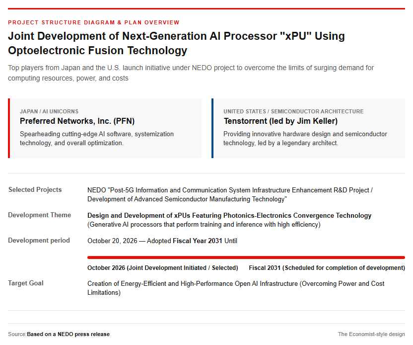
Amid the exponential increase in demand for computational resources driven by the rapid advancement of AI technology, a joint research framework has been launched between Preferred Networks, Inc. (PFN), a Japanese AI unicorn, and US-based Tenstorrent, led by legendary semiconductor architect Jim Keller. On October 20, 2026, the companies’ project was officially selected for the open-call theme “Design and Development of xPU Implemented with Opto-Electronic Convergence Technology” under the “Project for Enhanced Infrastructural Development of Post-5G Information and Communication Systems / Development of Advanced Semiconductor Manufacturing Technologies” of the New Energy and Industrial Technology Development Organization (NEDO). Throughout the development period up to fiscal 2031, this development project will pursue the systemization of the “xPU,” a processor for generative AI that executes both training and inference with extremely high efficiency. The significance of top-tier Japanese and American companies, which hold unique presences in the semiconductor industry, teaming up to embark on full-scale joint research and development under a national project is immense. As shown in the diagram below, the development of next-generation processors will serve as the foundation supporting the future advanced AI society.
The Social Background Behind Breaking NVIDIA’s Monopoly and Escaping HBM Dependency
In the current AI infrastructure market, U.S.-based NVIDIA’s GPUs reign as the de facto standard, but the severe increase in power consumption, soaring product prices, and shortages of High Bandwidth Memory (HBM) have become major structural challenges for the entire industry. As pointed out in the revised “Semiconductor and Digital Industry Strategy” published by Japan’s Ministry of Economy, Trade and Industry (METI) in June 2026, the axis of competition is shifting from an approach that relies solely on the computational performance of standalone AI models to comprehensive and operational capabilities that encompass power efficiency and communication infrastructure. The rapid surge in power consumption within data centers places an immense burden on the global environment and power grids, and we are facing unsustainable limits on the extension of conventional semiconductor architectures. Amidst these circumstances, there is a strong global demand for the establishment of domestic and open AI computing infrastructures based on new design philosophies that do not excessively rely on existing high-end GPUs or expensive HBM configurations.
Technological Innovation Pioneered by Optoelectronic Convergence and RISC-V
Ultra-High Bandwidth and Energy Efficiency Enabled by 3D Memory Integration and Optoelectronic Fusion
At the core of this joint development project is the integration of optoelectronic fusion technology, which performs communication by replacing a portion of electrical signals with optical signals, and cutting-edge packaging technology. By utilizing optical transmission, it achieves a dramatic reduction in power consumption, low-latency, and high-capacity communication compared to conventional electrical wiring, thereby resolving the bottlenecks of large-scale computing spanning multiple nodes. In hardware development, the division of roles is clearly defined, and PFN is in charge of 3D memory packaging technology applying cutting-edge processes. By adopting a 3D stacked structure in which storage devices (DRAM) are directly placed and stacked vertically on top of arithmetic units (logic) that process data, the plan is to secure ultra-high memory bandwidth that surpasses conventional GPUs while significantly reducing manufacturing costs compared to HBM.
The Open RISC-V Architecture and the Strengths of Division of Labor
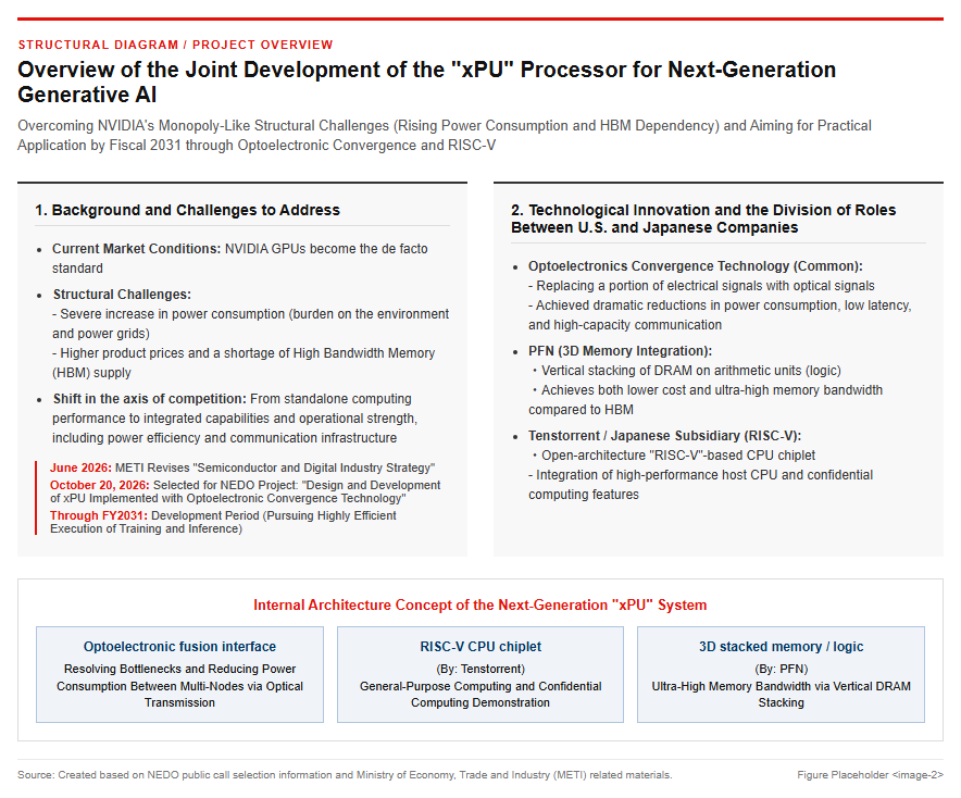
Meanwhile, Tenstorrent is responsible for developing CPU chiplets based on the open architecture “RISC-V,” which utilizes cutting-edge processes. By integrating the high-performance host CPU technology and advanced confidential computing functions the company has cultivated, it will provide a highly secure general-purpose computing infrastructure. In addition, its Japanese subsidiary, Tenstorrent Japan, will be in charge of the specific design of the CPU chiplets and software development for confidential computing verification. By adopting an open instruction set that is not tied to a specific proprietary vendor, developers will be enabled to perform custom designs with a high degree of freedom, dramatically improving the transparency and scalability of the software development ecosystem. The internal configuration image of the next-generation xPU is scheduled to be designed as follows.
Future Roadmap and Outlook for Social Implementation
Research and Development Toward Fiscal Year 2031 and Collaboration Framework with Academic Institutions and Industry
Promoted as a NEDO project, this initiative has a research and development period set through fiscal year 2031, aiming for prompt commercialization and practical application upon completion. To build highly effective foundational technologies, a close cooperative framework has been established with top-class domestic universities and research institutions as sub-contractors. Specifically, the University of Tokyo, Kobe University, Toyo University, the Japan Agency for Marine-Earth Science and Technology (JAMSTEC), and the Japan Atomic Energy Agency (JAEA) are participating, advancing the research and development of applications specialized in cutting-edge fields in parallel. Through a vertically integrated model of industry-academia-government collaboration that combines the strengths of the academic and industrial worlds, a system is in place to seamlessly cover everything from basic theory to actual system construction and demonstration testing.
The Future of Industry Transformed by Physical AI and Scientific Research
The next-generation xPU processors under development are envisioned for deployment in society not only for on-screen language processing, but across a wide variety of real-world industrial domains. Specifically, the main target fields include “Physical AI” to drive robotics, autonomous driving, and smart manufacturing; “AI agents” capable of advanced autonomous reasoning; and “AI for Science,” which dramatically accelerates material discovery, weather forecasting, and drug discovery simulations. The overwhelming computing power enabled by ultra-power-saving optoelectronic convergence and high-bandwidth memory is expected to fundamentally boost Japan’s international competitiveness in the manufacturing, materials, chemicals, and medical fields, serving as a robust technological foundation to support future critical infrastructure.
Reference page
- [Preferred Networks Inc. News Release] https://www.preferred.jp/ja/news/1791
- [NEDO Project Selection Notice] https://www.nedo.go.jp/koubo/IT3_100387.html
【#AISemiconductors #PFN #Tenstorrent #PhotonicsElectronicsConvergence #RISCV #NextGenerationxPU】

コメント