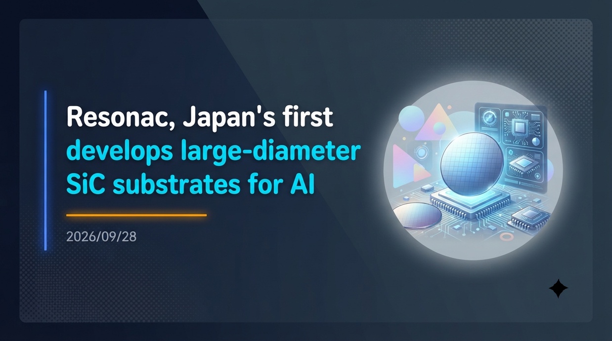
Resonac has succeeded in the single-crystal growth and substrate processing of SiC (silicon carbide) with a diameter of 300 mm (12 inches), making it one of the largest in the world. In the background are challenges such as curbing power consumption in data centers associated with the rapid expansion of generative AI and severe heat generation in AI server semiconductors, leading to growing expectations for it as a new material that goes beyond existing power semiconductor applications.
- One of the world’s largest 12-inch single-crystal growth and processing
- Advantages and Productivity Over Conventional 6-inch and 8-inch Substrates
- Physical Limits and Thermal Challenges Facing Generative AI Data Centers
- Developing new applications for heat dissipation substrates and advanced packages
- Strengthening the domestic production system and public-private partnership through NEDO projects
- Future Developments and Key Focus Areas in the Semiconductor Materials Market
One of the world’s largest 12-inch single-crystal growth and processing
On September 15, 2026, Resonac Corporation announced that it has successfully grown single crystals and processed substrates of 300 mm (12 inches) in diameter—one of the largest sizes in the world—for silicon carbide (SiC), a next-generation electronic material. This development achievement utilizes partial results from the “Development of Wafer Technology for Next-Generation Power Semiconductors” project, a Green Innovation Fund project promoted by the New Energy and Industrial Technology Development Organization (NEDO).
Compared to conventional silicon (Si) substrates, SiC features the ability to significantly reduce energy loss and heat generation during power conversion. While adoption has progressed primarily in electric vehicles (EVs) and renewable energy equipment, achieving larger diameters has posed extremely high hurdles in terms of maintaining crystal uniformity and defect control technology. By bringing together the crystal growth and processing technologies that Resonac has cultivated over many years, an important technological milestone toward future larger diameters and higher quality has been established.
The following figure shows a technical illustration of the 300mm SiC single-crystal substrate that has achieved a larger diameter.
Advantages and Productivity Over Conventional 6-inch and 8-inch Substrates
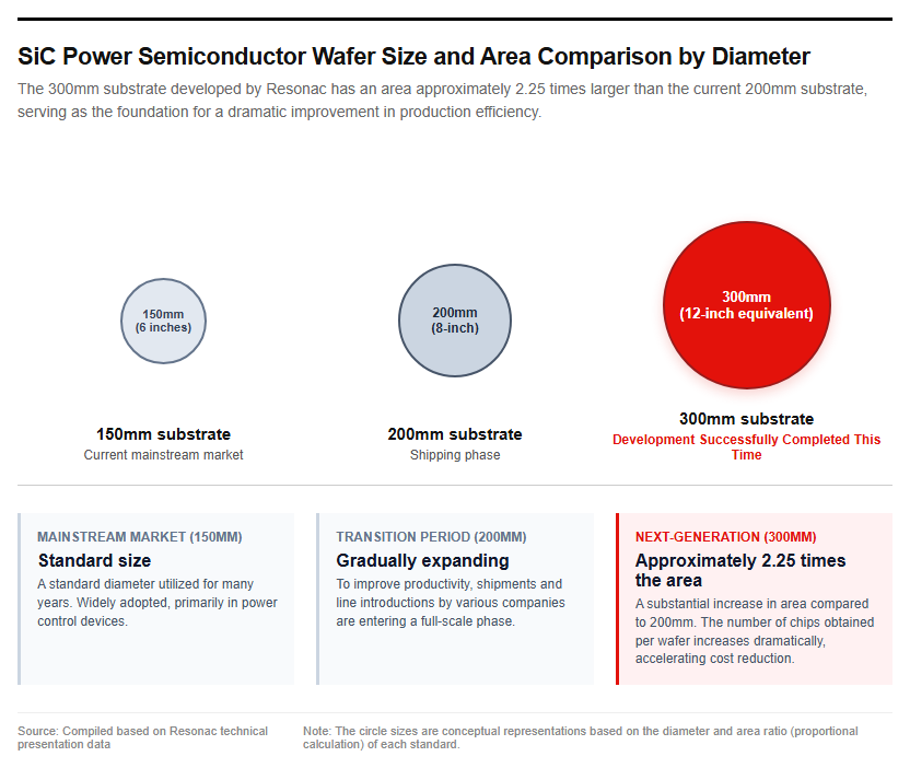
In the semiconductor materials market, 150mm (6-inch) SiC epitaxial wafers are currently the mainstream, and shipments of 200mm (8-inch) products are also beginning. The 300mm substrate recently developed by Resonac reaches approximately 2.25 times the area of a 200mm substrate when comparing the areas of circular substrates.
Achieving larger-diameter substrates dramatically increases the total number of chips that can be manufactured and harvested from a single wafer, which is expected to improve production efficiency on semiconductor manufacturers’ production lines and reduce manufacturing costs.
The main benefits of increasing the diameter are as follows:
- A significant increase in the number of chips obtained from a single wafer
- Potential for utilizing knowledge and equipment concepts from existing 300mm silicon manufacturing lines
- Acceleration of market penetration through reduced manufacturing costs per chip
Productivity improvements will be a key factor in strongly supporting a stable supply to meet the rapidly growing demand for power semiconductors and the advanced electronics sector.
The Importance of SiC Substrates and Thermal Management in the AI Era
Physical Limits and Thermal Challenges Facing Generative AI Data Centers
With the rapid evolution of generative AI and large language models (LLMs), the computing power of AI chips, led by NVIDIA, is increasing dramatically. To process vast amounts of data in an extremely short time, multiple chips are densely integrated using advanced packaging technologies such as high-bandwidth memory (HBM) and 2.5D packaging.
However, with increasing density and full-scale operation, the generation of extremely intense heat inside semiconductor packages has become a serious bottleneck. In multilayer structures where multiple layers of dissimilar materials with different expansion rates are laminated together, exposure to high temperatures creates mutual pulling forces, leading to the physical distortion and warping of substrates and chips in the sub-millimeter micro-world. This problem of heat and warping, which causes circuit disconnections and connection failures, has become a major barrier preventing advanced semiconductors from achieving their full performance.
Developing new applications for heat dissipation substrates and advanced packages
Single-crystal SiC possesses high thermal conductivity that dissipates heat extremely efficiently, in addition to functioning as a power semiconductor device for power control. Focusing on this thermal property, Resonac is eyeing its potential application to heat dissipation substrates for semiconductors used in AI servers and high-performance computing (HPC)—which are generating increasingly high amounts of heat—as well as advanced package substrates.
In addition, since SiC has the optical property of a high refractive index, its application is also envisioned in the field of optical devices such as AR (augmented reality) smart glasses. Beyond the conventional power control domain, its application is expected to expand into the following new fields.
- High-Efficiency Heat Dissipation Substrate for AI Accelerators and HPC
- Structural Materials for Suppressing Distortion and Warpage in Advanced Packaging
- High-Refractive-Index Optical Substrates for Next-Generation AR Smart Glasses
This is driving the creation of new demand for the material as an innovative solution that improves both power conversion efficiency and thermal management.
The figure below illustrates the concept of thermal management structures in AI servers and advanced packaging.
Resonac’s Business Strategy and Future Outlook
Strengthening the domestic production system and public-private partnership through NEDO projects
Resonac positions SiC epitaxial wafers as a core growth business and is rapidly advancing the establishment of a stable domestic supply chain. At the Yamagata Plant of Resonac Hard Disk Corporation (Higashine City, Yamagata Prefecture), a new production building with a building area of approximately 5,832 square meters has been constructed, and a completion ceremony was held on September 12, 2025. Following equipment installation, this facility is scheduled to begin operations in 2026.
This capital investment is part of the “Plan for Securing Supply of Specified Critical Materials (SiC Wafers)” certified by the Ministry of Economy, Trade and Industry (METI) on June 16, 2023, under the Economic Security Promotion Act. Leveraging government policy support and NEDO’s technology development projects, the public and private sectors are working together to strengthen the domestic semiconductor supply chain.
Future Developments and Key Focus Areas in the Semiconductor Materials Market
While the SiC power semiconductor market is facing changing conditions—such as a short-term slowdown in EV demand in Europe and the United States and the rise of competitors—power supply demand for AI data centers and new applications for advanced packaging are rapidly emerging as new growth drivers.
The key points to focus on in future business development are as follows.
- Establishment of High-Quality Manufacturing Technology for 300mm SiC Single Crystal Substrates and Concretization of the Future Mass Production Roadmap
- Expanding supply capacity for 8-inch substrates and other products through the new building at the Yamagata Plant, scheduled to begin operations in 2026.
- Expanding market share through long-term supply contracts with major global manufacturers such as Germany’s Infineon Technologies
- Provision of comprehensive matching solutions with back-end materials through advanced packaging consortia such as “JOINT”
Resonac is driving its transformation from a chemical manufacturer into an innovation company in semiconductors and electronic materials, and is expected to further enhance its competitiveness in the global market, centered on large-diameter SiC substrate technology.
Reference page
- 【Resonac Corporation News Release (Development of 300mm SiC Single Crystal Substrates)】https://www.resonac.com/jp/news/2026/09/15/4015.html
- [Resonac Corporation News Release: Completion of SiC Epitaxial Wafer Production Building at Yamagata Plant] https://www.resonac.com/jp/news/2025/09/16/3614.html
【#Resonac #SiCSubstrates #AISemiconductors #PowerSemiconductors #300mmWafers #ThermalManagement #AdvancedPackaging】
コメント