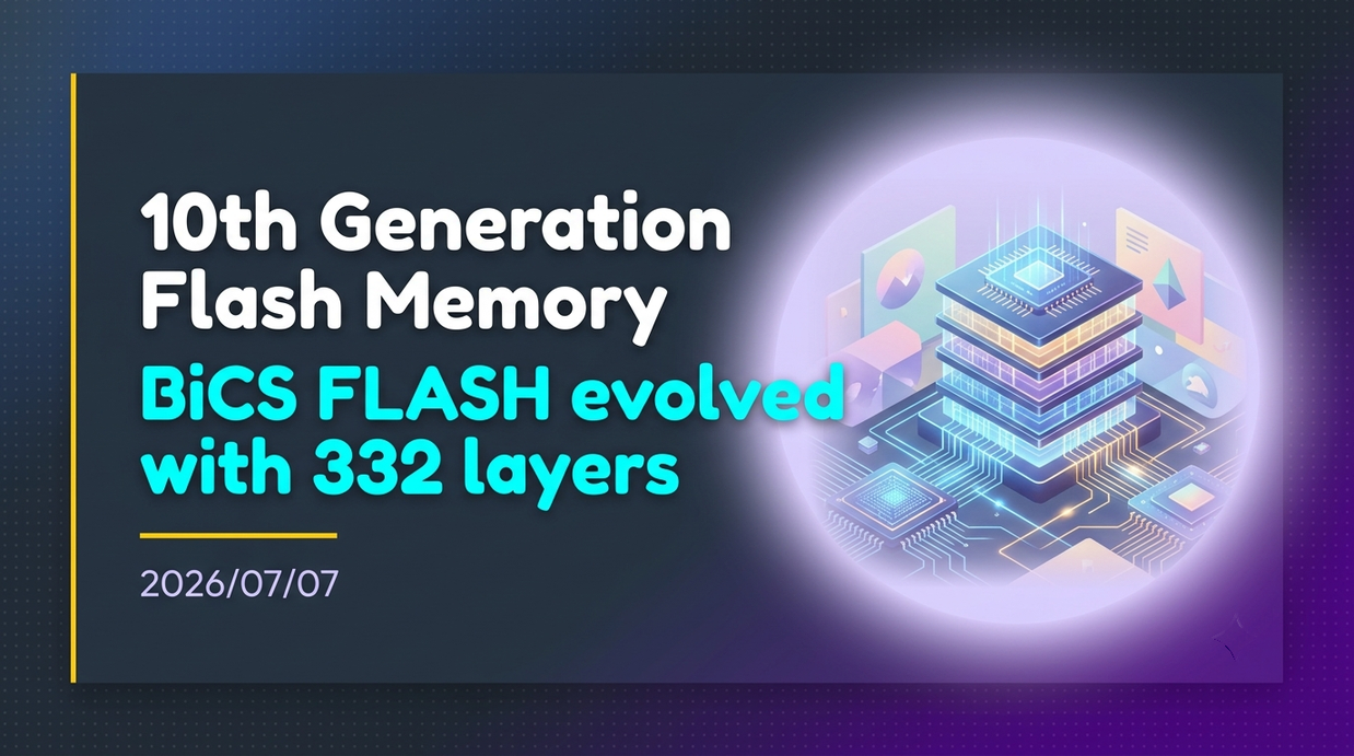
Kioxia has begun sample shipments of products applying 10th generation 3D flash memory technology. Driven by the explosive demand for large-capacity, low-power storage in AI data centers, it will play a central role in next-generation infrastructure.
- Dramatic Improvement in Bit Density with 332 Layers
- Evolution of interface speeds to achieve 4.8Gbps
- Latest supply system at Kitakami Plant’s Second Production Building
- Stock price surged over 10 percent after sample shipment announcement
- Transformation to an astonishing profit structure boasting a 74% profit margin
- Cost and reliability optimization by avoiding excessive stacking
- A dual-axis strategy covering both high performance and large capacity
- Redefining storage through collaboration with NVIDIA
- Mass Production Start in 2027 and Laying the Groundwork for Next-Generation Technologies
Dramatic Improvement in Bit Density with 332 Layers
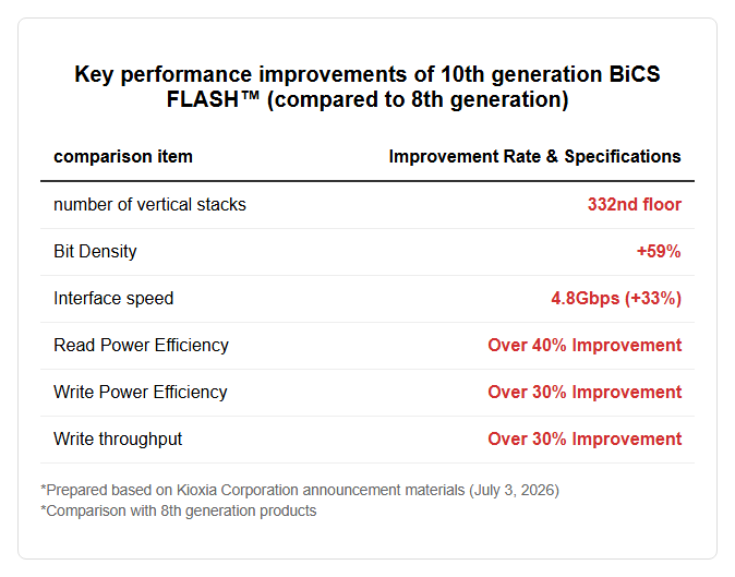
On July 3, 2026, Kioxia Corporation announced that it has begun sample shipments of a 1TB capacity TLC (Triple-Level-Cell) product applying BiCS FLASH, the 10th generation 3D flash memory technology. The biggest feature of this latest generation is the increased vertical stacking count to 332 layers. This has succeeded in improving bit density by 59 percent compared to the conventional 8th generation.
In the evolution of flash memory, increasing density—how to pack a large amount of data into a limited area—is a crucial metric directly linked to cost competitiveness. This 10th generation product achieves industry-leading bit density by best mixing proprietary planar shrinking technology with advanced vertical stacking technology. Please refer to the diagram below.
This technological innovation is especially powerful on large-scale computing infrastructures such as AI data centers. With the spread of generative and agentic AI, the datasets handled are rapidly growing in size, making it possible to implement large-capacity storage within limited server rack space, posing a major challenge. Kioxia’s 10th generation BiCS FLASH provides a clear answer to this demand for higher density, helping to improve implementation density and optimize total cost of ownership in data centers.
Evolution of interface speeds to achieve 4.8Gbps
Another significant evolution of the 10th generation BiCS FLASH is the dramatic improvement in data transfer speed. This product achieves 4.8 gigabits per second in NAND interface speed, a 33% improvement compared to the 8th generation. Supporting this acceleration is Kioxia’s innovative wafer bonding technology CBA (CMOS directly Bonded to Array), which has been introduced since the 8th generation.
CBA technology is a method in which wafers formed by memory cell arrays and wafers formed by CMOS circuits are manufactured separately, and these are then laminated. This enables optimal heat treatment for the circuit section, breaking through physical limitations that hinder high-performance interfaces. Additionally, OPS (On Pitch Select Gate Drain) technology, which removes unused memory holes to shorten bitlines and reduce word line capacity, is also utilized.
In AI systems, the large data transfers between processors and storage often become bottlenecks, and improving interface speed directly impacts overall system performance. Especially in next-generation architectures proposed by partners like NVIDIA, which define SSDs as an extended memory layer for GPUs, this high-speed transfer performance of 4.8Gbps will play an extremely important role. Kioxia has put CBA technology into practical use ahead of its competitors, and in this 10th generation, it fully demonstrates its technological advantages.
Latest supply system at Kitakami Plant’s Second Production Building
Production of the newly announced 10th generation products will take place in the second manufacturing building (K2 building) of the Kioxia Kitakami Factory located in Kitakami City, Iwate Prefecture. This K2 building is a state-of-the-art manufacturing facility that just began operations in September 2025, serving as the world’s only facility capable of expanding production of 332-layer flash memory. Kioxia has built this large-scale production capacity in collaboration with its long-standing partner, SanDisk in the United States.
The start of production at Building K2 of the Kitakami factory carries strategic significance to alleviate concerns about supply shortages caused by the rapid expansion of AI demand. By the end of fiscal year 2026, about 80 percent of Kioxia’s total bit output is planned to switch to the latest technologies from the 8th generation onward, with the 10th generation products playing a central role. With the start of sample shipments, evaluation and validation by major hyperscaler and server manufacturers are expected to progress, accelerating the transition to mass production.
Additionally, Kioxia places great importance on the efficiency of capital investment, planning an average annual investment of approximately 470 billion yen over the next three years. This represents an increase of about 60 percent compared to fiscal year 2025, but by utilizing the latest equipment at the Kitakami plant, we aim to produce at bit-unit prices lower than the industry average. By simultaneously advancing technological innovation and expanding production scale, Kioxia is aiming to solidify its solid position in the rapidly evolving AI market supply chain.
[Impact on Market and Stock Prices] Capital Market Evaluation and Financial Improvement
Stock price surged over 10 percent after sample shipment announcement
On July 3, 2026, Kioxia’s stock price reacted dramatically following the announcement of its 10th generation products. At the start of trading, due to heavy upside on the Nikkei Stock Average and fluctuations in market sentiment, the company’s stock price initially fell by more than 9 percent. However, as the specific specs and technical details of the new product were digested by the market, buying surged and the stock price quickly reversed into positive territory.
Ultimately, the stock price on that day surged by more than 10 percent compared to the previous day, trading at an extremely high level of 83,940 yen. The capital markets have evaluated the overwhelming bit density and improved power efficiency of this 10th generation BiCS FLASH as decisive factors determining future profitability. In particular, the storage market’s booming momentum, driven by AI demand, is expected to continue into 2027, and expectations that Kioxia’s technological leadership will lead to medium- to long-term performance growth have driven up stock prices.
Prior to this, Kioxia had already established its position as a leading semiconductor company in both name and reality, surpassing Toyota Motor Corporation to become Japan’s top semiconductor company thanks to the AI boom. This technology announcement served as an opportunity to reaffirm to investors that growth is based on tangible technological capabilities, not just a temporary boom.
Transformation to an astonishing profit structure boasting a 74% profit margin
The most recent financial indicators presented by Kioxia have overturned the conventional wisdom of former semiconductor manufacturers. In the guidance for the first quarter of fiscal 2026, we achieved an impressive operating profit margin (ROS) of 74 percent. This is due to strong sales of high value-added SSD products for AI data centers, combined with rising memory prices and thorough cost reductions. Please refer to the diagram below.
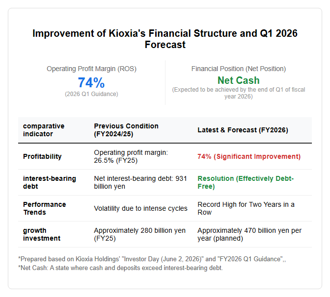
The company has achieved record highs in revenue and operating profit for two consecutive years, aiming to break away from a business model that was heavily swayed by economic cycles in the past. The result of strategically shifting our business portfolio from cyclical growth centered on the consumer market to stable growth driven by the AI infrastructure market is reflected in this exceptionally high profit margin.
Additionally, this strong cash generation has led to rapid repayment of interest-bearing debt. By the end of the first quarter of fiscal year 2026, cash and deposits are expected to achieve a net cash position exceeding interest-bearing debt. Following the dramatic improvement in financial soundness, from fiscal year 2027, we are actively considering profit returns to shareholders, including the launch of a progressive dividend policy, laying a solid foundation for balancing growth investment and shareholder returns.
[Background of Management and Strategy] The ‘332 layers’ as the optimal solution
Cost and reliability optimization by avoiding excessive stacking
In the 10th generation BiCS FLASH, Kioxia set the number of layers at 332 due to advanced management decisions that do not simply follow the simple stacking of layers. In the semiconductor industry, there is a trend to compete for stacking with over 400 layers, but if the number of layers increases excessively, capital investment and the number of manufacturing processes will skyrocket, resulting in higher manufacturing costs per wafer.
According to Kioxia’s estimates, by keeping the number of layers at 332 and combining planar reduction techniques in a balanced way, the bit price can be reduced by about 10% compared to aiming for over 400 layers. Furthermore, excessive multilayer processing forces the physical thinning of memory cells, reducing the amount of charge they can hold and raising concerns about data reliability. By selecting 332 layers in the 10th generation, we succeeded in maintaining about a 35 percent advantage in cell reliability.
This strategy of targeting the point where performance, cost, and reliability harmonize at the highest level symbolizes the company’s technological leadership. Rather than simple spec competition, the core of the 10th Generation design philosophy lies in a development approach that emphasizes economic rationality and operational stability that customers as data center operators truly seek.
A dual-axis strategy covering both high performance and large capacity
Kioxia has adopted a dual-axis strategy in product development to meet the needs of a diversified market. The first core is the pursuit of large capacity and high density that the newly announced 10th generation and the upcoming 11th generation will pursue. This mainly targets SSDs for enterprise and data center markets, where massive amounts of data need to be accumulated.
The other focus is on our product lineup, which pursues ultimate high performance by intentionally limiting the number of layers. This is defined as development code generation 9 or Y generation, targeting AI-powered PCs, mobile devices, or specialized storage applications requiring low latency. By reducing stacking, it enables integration with more advanced peripheral circuits (CMOS), achieving the fastest response performance.
This dual-axis strategy aims to establish a position of “providing optimal memory at every layer of AI systems.” By timely introducing optimal solutions tailored to each application—such as overwhelming capacity in some areas and extreme response performance in others—the company is prepared to maintain a multifaceted technological advantage over overseas competitors like Samsung Electronics and SK Hynix.
[Future Developments & Points to Watch] Becoming an infrastructure provider company for the AI era
Redefining storage through collaboration with NVIDIA
The 10th generation BiCS FLASH is heading beyond just SSDs as data storage locations. Together with its key partner NVIDIA, Kioxia is strongly advancing the concept of redefining storage as an extended memory layer for GPUs. This concept utilizes ultra-high-speed, large-capacity SSDs as storage destinations for KV caches that store past computation results and vast vector databases required for RAG (Search Extension Generation).
Especially in systems like agentic AI, where AI autonomously performs inferences, the frequency of data read/write and processing density increase dramatically. Kioxia plans to merge the boundaries between processors and storage through its next-generation SSD lineup based on 10th generation technology, aiming to optimize the entire system.
This allows areas previously covered only by HBM (Wide Band Memory) to be supplemented by more affordable, high-capacity flash memory. As storage evolves into a core component that determines the computing performance of AI systems, Kioxia will further expand its role as a technology partner supporting the core of AI infrastructure, beyond just a component supplier.
Mass Production Start in 2027 and Laying the Groundwork for Next-Generation Technologies
The 10th generation BiCS FLASH, for which sample shipments have begun, is expected to begin mass production at the Kitakami plant in 2027. With the full-scale market launch of this product, the power saving and large-capacity expansion of AI data centers will accelerate even further. In particular, the 30% improvement in power efficiency during readout will be an extremely attractive incentive for data centers worldwide facing severe power shortages.
While Kioxia is advancing mass production of this 10th generation, it has already begun developing innovative technologies such as the next-generation 11th generation BiCS FLASH and beyond. At the research level, we have successfully demonstrated operations such as horizontal channel flash memory (HCF) with optimized cell stacking directions and three-dimensional oxide-semiconductor channel transistor technology, paving the way for further future evolution.
Additionally, with the goal of the end of fiscal year 2027, there are plans to establish a (tentative name) Kioxia College to cultivate highly specialized personnel. Can we strengthen the three pillars of technology, finance, and talent to lead the semiconductor supercycle toward 2030? Sample shipments of 10th-generation products are drawing significant attention as the first step toward realizing this ambitious roadmap.
[#キオクシア #BiCSFLASH #AI半導体 #データセンター #332層 #SSD #ネットキャッシュ]

コメント