Toyobo has stepped up its proposal of polyimide films for interposers used in semiconductor chiplets. This move comes amid rapidly surging demand for advanced packaging technologies that integrate heterogeneous chips at high density, driven by the spread of generative AI and the need for higher semiconductor performance.
- Key Highlights and Development Background of Interposers for Chiplets
- Technical Advantages of the High Heat-Resistant Polyimide Film “XENOMAX”
- Thermal Expansion Mismatch in Heterogeneous Integration and the Need for Silicon-Equivalent CTE
- Substrate Warpage Suppression Mechanism via 500°C Heat Resistance and High Modulus
- Adoption in Next-Generation Package Substrates via Co-Creation Platforms
- Medium-Term Growth Prospects Driven by AI Server and Beyond 5G Expansion
Key Highlights and Development Background of Interposers for Chiplets
Toyobo, along with its group companies Toyobo MC Corporation and XENOMAX JAPAN CO., LTD., is aggressively promoting high-performance polyimide films for chiplet architectures, which are becoming the centerpiece of next-generation semiconductor manufacturing. The overarching driver is the imperative to achieve higher functionality and processing capability in semiconductors, fueled by growing demand for generative AI servers and expectations for the adoption of next-generation communication standards such as Beyond 5G and 6G. Historically, semiconductor performance gains were driven by miniaturization technology—shrinking circuit wiring on silicon wafers. However, physical limits and soaring manufacturing costs have created a bottleneck, making it difficult to improve performance within a single monolithic chip. Consequently, 2.5D and 3D packaging technologies have attracted significant attention, enabling the high-density integration and bonding of multiple functional semiconductor chips (chiplets) onto a single substrate. The Toyobo Group is proposing its proprietary polyimide film technology as an insulating material for interposers—which connect these chiplets—as well as for package substrates. At “SEMICON Japan 2025,” an international exhibition held at Tokyo Big Sight from December 17 to 19, 2025, the group showcased these development products for the first time, emphasizing early commercialization and expanded adoption across the semiconductor industry.
Technical Advantages of the High Heat-Resistant Polyimide Film “XENOMAX”
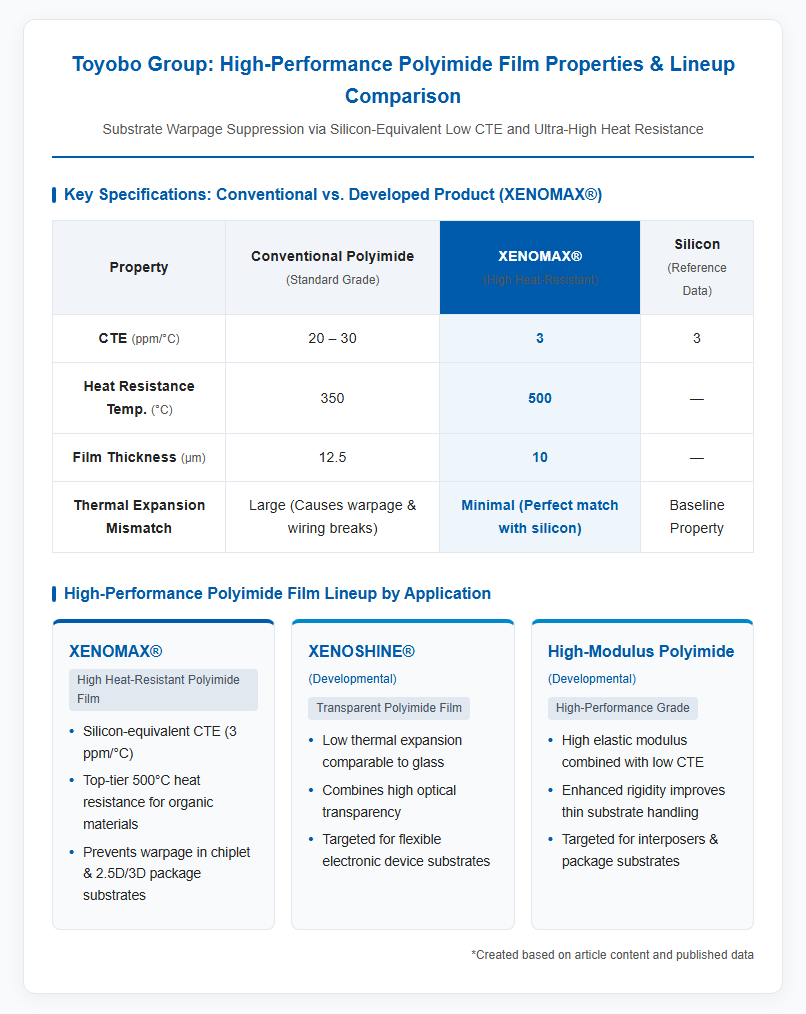
Toyobo’s high heat-resistant polyimide film “XENOMAX” possesses revolutionary properties that significantly enhance substrate adhesion and reliability. This breakthrough stems from the fusion of the company’s long-cultivated polymer synthesis expertise and precision film-forming technology, achieving physical properties in an organic material that rival those of inorganic materials. While conventional organic polyimide films offer excellent flexibility, they suffer from a key drawback: significant dimensional changes when subjected to heat. XENOMAX, however, combines exceptional dimensional stability with extremely high heat resistance, making it an ideal specification for insulating materials in advanced semiconductor packages requiring ultra-fine wiring structures. Furthermore, the Toyobo Group has added to its lineup a high-performance polyimide development film that offers low thermal expansion combined with a higher elastic modulus than standard polyimide films, targeting applications in interposer substrates. The group is also expanding its portfolio with transparent polyimide films such as “XENOSHINE,” which boasts a low coefficient of thermal expansion comparable to glass while maintaining optical clarity, establishing a framework to address diverse demands across flexible electronic devices and cutting-edge semiconductor packaging. The diagram below illustrates the physical property characteristics of these development products.
Thermal Management and Dimensional Stability Challenges Facing Advanced Semiconductor Packaging
Thermal Expansion Mismatch in Heterogeneous Integration and the Need for Silicon-Equivalent CTE
In advanced semiconductor packaging, thermal management and substrate warping pose the greatest engineering challenges. This issue is driven by the increasing amount of heat generated by highly integrated silicon chips, combined with the structural tendency for internal stress and strain to arise from thermal expansion mismatches when combining materials with different physical properties. In chiplet architectures and multi-layer stacks of High Bandwidth Memory (HBM)—such as 12-layer or 16-layer configurations—differences in material thermal expansion occur during thermal processing steps and device operation. When this expansion differential concentrates at the joints between the silicon chip and the insulating film, or on ultra-fine circuit traces (with line/space dimensions of 15/15 μm or less, and even 10/10 μm or less), it can cause micro-cracks in fine bumps or, in the worst case, electrical open circuits, severely degrading product yield. Consequently, insulating materials used in state-of-the-art packaging require an exceptionally high degree of dimensional stability that prevents dimensional changes across repeated heating and cooling cycles.
Substrate Warpage Suppression Mechanism via 500°C Heat Resistance and High Modulus
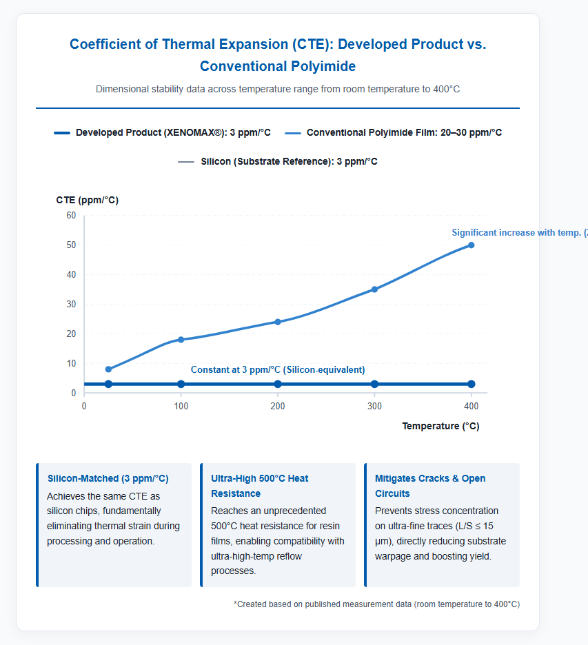
The primary numerical benchmark demonstrating Toyobo’s technological rationale is XENOMAX’s outstanding dimensional stability, characterized by a coefficient of thermal expansion (CTE) of 3 ppm/°C that remains virtually unchanged from room temperature to over 400°C. Conventionally, standard polyimide films had CTE values of approximately 20 to 30 ppm/°C, creating a substantial expansion mismatch against silicon chips (which have a CTE of approximately 3 ppm/°C) during thermal processing. By matching the CTE of silicon, XENOMAX succeeds in reducing thermal-expansion-induced strain to near zero during thermal processing. This fundamentally mitigates the risks of wiring cracks and open circuits in chip-on-film and interposer substrates. In addition, the product achieves a top-tier heat resistance temperature of 500°C, an unprecedented level for organic insulating films. This capability allows the material to withstand ultra-high-temperature semiconductor manufacturing processes and reflow steps without thermal degradation, overcoming the limitations of conventional resin materials. The following graph compares the CTE of XENOMAX with that of conventional films.
Market Trends in Semiconductor Materials and Toyobo’s Future Outlook
Adoption in Next-Generation Package Substrates via Co-Creation Platforms
To accelerate the adoption of advanced semiconductor packaging materials, “co-creation development” involving device manufacturers, foundries, and equipment suppliers is rapidly expanding across the industry. As 2.5D/3D packages and panel-level packages (such as 515 × 510 mm panel sizes) grow larger and more complex, satisfying demanding performance requirements with a single standalone material has become increasingly difficult. This necessitates holistic optimization across materials, process conditions, and equipment from the initial design phase. Co-creation evaluation platforms like “JOINT3,” led by Resonac, involve numerous participating companies from Japan and abroad, utilizing near-commercial production structures to expedite development. Within the Toyobo Group, alongside high heat-resistant polyimide films, a comprehensive suite of backend bonding and insulating materials—including cureless high-heat-resistant adhesive films and organic-solvent-soluble polyphenylene ether (PPE) materials—is being developed to secure standard-setter positions through industry evaluation platforms and consortiums.
Medium-Term Growth Prospects Driven by AI Server and Beyond 5G Expansion
Under its long-term vision “Sustainable Vision 2030” and the “2030 Medium-Term Management Plan,” Toyobo positions its advanced materials business—centered on high-performance films—as its top-priority growth driver. Reflecting on past earnings sluggishness and delayed structural reforms, the company is shifting its strategic direction from volume-driven growth to margin-driven profitability (“from quantity to quality”), executing a business portfolio transformation that concentrates management resources on high-value-added advanced materials. Toyobo has set ambitious financial targets for FY2030, including an ROE exceeding 8%, net sales of 500 billion yen, and operating profit of 45 billion yen (an operating margin of 9.0%). Polyimide films and interposer materials for semiconductor backend processes are expected to serve as major profit growth drivers in reaching these goals. With the global rise of AI servers and high-performance computing, Toyobo’s polyimide film technology—combining silicon-level dimensional stability with ultra-high heat resistance—is poised to strengthen its presence as an indispensable foundational technology supporting the evolution of the semiconductor industry.
Reference Pages
- [Toyobo Co., Ltd. SEMICON Japan 2025 Special Page] https://www.toyobo.co.jp/event/semicon2025/
- [Toyobo MC Corporation Press Releases] https://www.toyobo-mc.jp/news/
【#Toyobo #Semiconductor #PolyimideFilm #Chiplet #XENOMAX #AdvancedPackaging #ScienceAndTechnology】


コメント