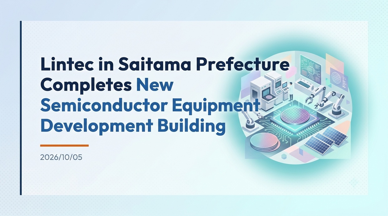
Lintec has completed construction of a new “R&D Building” at its Ina Technology Center in Ina-machi, Kitaadachi-gun, Saitama Prefecture, investing approximately 2.5 billion yen, and operations began in October 2026. This is in response to the booming demand for semiconductor-related equipment driven by the rapid expansion of the generative AI market, with the aim of significantly enhancing manufacturing and development capabilities.
- Overview of the New Building Built with a 2.5 Billion Yen Investment and the Background of Its Launch
- A Reallocation Mechanism Achieving a 1.5x Development Area and 1.6x Manufacturing Area
- Rapid expansion of the semiconductor market and strengthening ability to meet short delivery time needs
- The Importance of Special Adhesive Tape Application and Peeling Equipment and HBM Manufacturing Equipment
- The Strengths of the “Total Proposal” Providing Materials and Equipment as an Integrated Package
- Synergy with Saitama City’s “Advanced Development Center”
- Future Outlook for Production and Development Systems for Next-Generation Semiconductor Packaging
Overview of the New Building Built with a 2.5 Billion Yen Investment and the Background of Its Launch
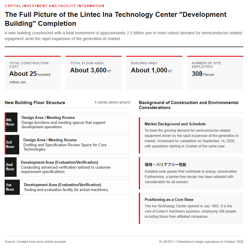
Lintec has built a new “Development Building” with a total construction cost of approximately 2.5 billion yen at the Ina Technology Center (Ina-machi, Kitaadachi-gun, Saitama Prefecture), which serves as a development and manufacturing base for various equipment. The facility was completed on September 14, 2026, and full-scale operations began in October of the same year. The completed development building boasts a four-story structure above ground, with a building area of approximately 1,000 square meters and a total floor area of approximately 3,600 square meters. In terms of floor structure, the first and second floors house development areas for evaluation and verification tailored to customer-requested specifications, while the third and fourth floors are equipped with design areas and meeting rooms. In addition, the new building features solar panels that contribute to energy conservation, as well as a state-of-the-art architectural design that incorporates barrier-free considerations. Opened in July 1983, the center is a core base for Lintec’s machinery business, with 308 employees—including temporary staff and affiliated company employees—working there as of September 2026. The completion of this new building was carried out as part of intensive capital investment to address the intensifying development competition and expanding demand for advanced semiconductors. As shown in the exterior image below, the design combines state-of-the-art environmental considerations with high functionality.
A Reallocation Mechanism Achieving a 1.5x Development Area and 1.6x Manufacturing Area
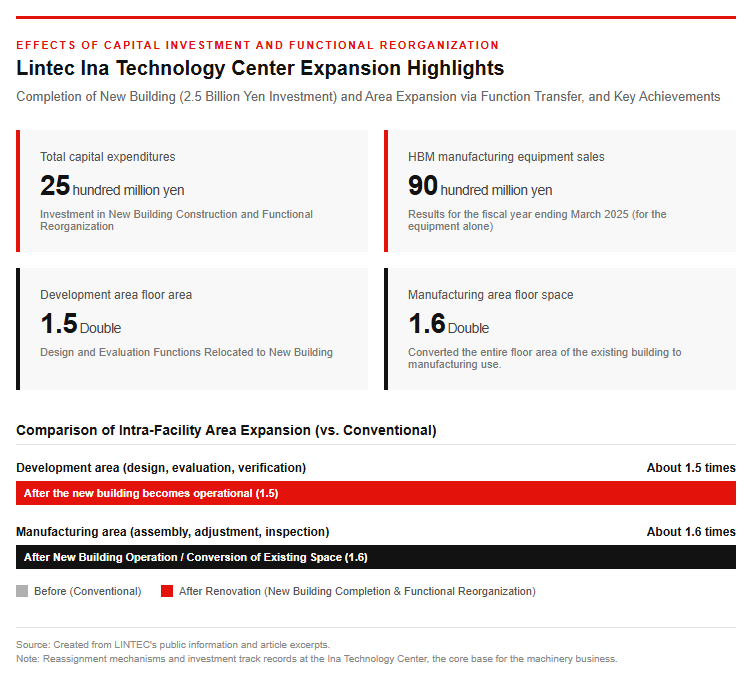
The greatest achievement of the recent construction of the new building lies in the smart functional reorganization and effective utilization of existing space accompanying the new facility. Previously, spaces dedicated to equipment design functions and evaluation/verification work tailored to individual customer requirements—which were handled in the existing building—were entirely relocated to the new building. This created a vast amount of empty space within the existing building, and its entire floor area was directly repurposed into a manufacturing area for assembling, adjusting, and inspecting semiconductor-related equipment. Through this layout rearrangement mechanism, the floor area of the development area across the entire Ina Technology Center has expanded to approximately 1.5 times its previous size. Simultaneously, the floor area of the manufacturing area for semiconductor-related equipment and other products has also significantly increased to about 1.6 times compared to before. Although the specific production volume of the equipment remains undisclosed, expanding the physical floor area of the manufacturing area by 1.6 times has successfully raised the upper limit of practical production capacity dramatically. A major distinctive feature is that it goes beyond simply adding floor area; it physically reorganizes and optimizes the flow lines for design/evaluation and assembly/manufacturing.
Rapid expansion of the semiconductor market and strengthening ability to meet short delivery time needs
Behind this ¥2.5 billion investment in capacity expansion lies the robust growth of the semiconductor market, driven by the rapid global expansion of AI demand. Lintec’s semiconductor-related equipment has maintained high operating rates in recent years, making it a regular occurrence for operations to push close to the limits of its conventional production capacity. Furthermore, amid the intense market fluctuations characteristic of the semiconductor industry, customer manufacturers have strongly demanded short delivery times, requiring the lead time from order to delivery to be minimized to the utmost limit. Because a shortage of production space could become a bottleneck against sudden requests to ramp up production, establishing a medium- to long-term stable supply system and building flexible supply capabilities had become urgent priorities. With the new building becoming operational in October and the expansion of existing manufacturing space, the company has secured the manufacturing capacity to respond swiftly even to sudden spikes in demand. Enhancing its capability to secure orders with short delivery times is a strategic imperative directly tied to maintaining and expanding market share, and the start of these operations is further elevating the company’s presence within the semiconductor supply chain.
Semiconductor-Related Equipment Handled by Lintec and Its Technical Role in Back-End Processes
The Importance of Special Adhesive Tape Application and Peeling Equipment and HBM Manufacturing Equipment
The semiconductor-related equipment developed and manufactured at the Ina Technology Center plays an extremely important role primarily in the back-end processes of semiconductor manufacturing. Specifically, its core products are equipment for applying and peeling special adhesive tapes used in the back-grinding process, where the backside of semiconductor wafers is ground to make them thinner, and the dicing process, where wafers are cut into individual chips. Representative equipment includes wafer mounters, tape laminators, tape removers, and UV irradiation systems. Furthermore, it also provides tape application equipment for DRAM stacking targeting the manufacturing process of High Bandwidth Memory (HBM), which is driving recent demand for generative AI, recording sales of approximately 9 billion yen from this equipment alone in the fiscal year ended March 2025. In advanced 3D packaging technologies represented by HBM and 3DIC, technology that applies and peels tape with ultra-high precision while preventing cracking and warping of ultra-thinned silicon wafers is essential. The configuration images of the semiconductor chips and equipment are shown below.
The Strengths of the “Total Proposal” Providing Materials and Equipment as an Integrated Package
The greatest strength of Lintec’s semiconductor business lies in its comprehensive proposal capability, which involves the in-house, integrated development and manufacturing of “materials (software)” in the form of high-performance adhesive tapes and “equipment (hardware)” to handle them. UV-curable dicing tapes and backgrinding tapes used in semiconductor back-end processes require sophisticated adhesive strength control, meaning they must hold firmly during processing yet peel off easily afterward. However, no matter how superior the adhesive tape may be, even the slightest deviation in equipment-side process conditions—such as mounting pressure, UV irradiation intensity, or peeling speed—can lead to wafer damage or decreased yields. By utilizing its proprietary equipment, Lintec establishes and offers customers optimal processes that draw out 100 percent of the material’s performance. Rather than simply selling machinery, the company provides standardized process specifications that highly integrate materials and equipment, thereby building a formidable barrier to entry that other companies cannot easily breach.
R&D Collaboration within Saitama Prefecture and Future Prospects for the Semiconductor Business
Synergy with Saitama City’s “Advanced Development Center”
Lintec’s semiconductor investments in Saitama Prefecture are not limited to the development building at the Ina Technology Center. The company established the “Advanced Development Center,” equipped with a cleanroom, investing a total of approximately 1.6 billion yen within the Advanced Technology Building of its research laboratory in Saitama City, Saitama Prefecture, and announced it in June 2026. The center is an advanced facility featuring ISO Class 5 and Class 7 clean environments, enabling material evaluation and process verification under conditions close to customers’ mass-production lines. While the Ina Technology Center is responsible for equipment design, manufacturing, and actual machine evaluation, the Saitama center handles the basic and applied development of low-contamination and low-residue tapes for chiplet technology and hybrid bonding. By closely cooperating, both bases in Saitama Prefecture have established a robust R&D and manufacturing network that seamlessly connects the development of cutting-edge materials to the design and mass production of specialized equipment to put them into practical use.
Future Outlook for Production and Development Systems for Next-Generation Semiconductor Packaging
Under its long-term vision “LSV 2030,” Lintec continues to make focused investments in growth areas such as semiconductor- and electronic component-related businesses. In addition to enhancing its facilities in Saitama Prefecture, the company is expanding its development and production infrastructure nationwide, including the opening of the “Tsukuba Innovative Creation Center”—a development base for carbon nanotube (CNT) pellicles for EUV exposure systems in Tsukuba, Ibaraki Prefecture—and the construction of the “Semiconductor Solutions Lab” (scheduled for completion in October 2028) in Itoshima, Fukuoka Prefecture, with an investment of approximately 20 billion yen. As semiconductor miniaturization approaches its physical limits, high-density packaging technologies such as 3D stacking and chiplet integration in back-end processes are growing increasingly important. With the new building at the Ina Technology Center now operational, the expansion to 1.6 times the equipment manufacturing capacity and 1.5 times the development area has been completed, establishing a framework to reliably capture the rapidly surging demand for HBM and next-generation packaging equipment. Moving forward, the company will continue to support the growth of the global semiconductor industry through total solutions that integrate materials and equipment.
Reference Page
- [Construction of a New Building at the Ina Technology Center | News Release | LINTEC Corporation]https://www.lintec.co.jp/topics/newsrelease/260929_a.html
- [Establishment of Advanced Development Center within Research Laboratory | News Release | LINTEC Corporation] https://www.lintec.co.jp/topics/newsrelease/260608_a.html
[#Lintec #SemiconductorEquipment #Saitama #InaTechnologyCenter #HBM #BackEndProcess #SemiconductorMaterials]


コメント