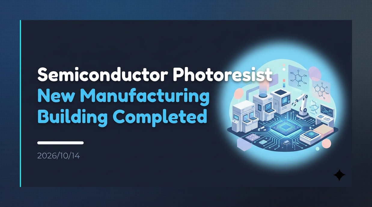
Tokyo Ohka Kogyo Co., Ltd. has completed a new manufacturing building for semiconductor photoresists at its Koriyama Plant in Koriyama City, Fukushima Prefecture, with an investment of approximately 23 billion yen, and operations are set to begin in November 2026. This development is driven by the need to strengthen the global supply system for EUV and ArF resists amid expanding demand for generative AI and advanced semiconductors.
- Completion and Operation Plan for the New Manufacturing Building with a 23 Billion Yen Investment
- The Complete Overview of Smart Factories Driving Automation and Digitalization
- The Role of Photosensitive Resins in Carving Circuits and EUV Lithography Technology
- The Strengths of Tokyo Ohka Kogyo, Boasting a 24.7% Global Market Share
- Expansion of the Global Production Base Based on the Medium-Term Management Plan
- Expansion of the Advanced Logic and AI Semiconductor Market and Key Points to Watch
Completion and Operation Plan for the New Manufacturing Building with a 23 Billion Yen Investment
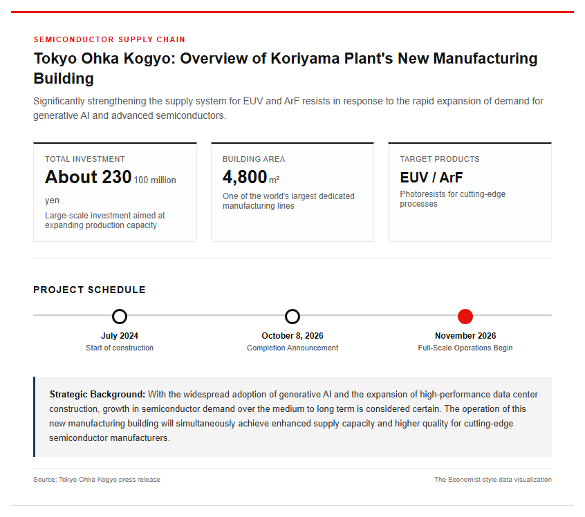
Tokyo Ohka Kogyo Co., Ltd. has completed a new manufacturing building for semiconductor photoresists at its Koriyama Plant located in Koriyama City, Fukushima Prefecture, and announced its completion on October 8, 2026. This facility was built to significantly expand the production capacity for high-performance materials, including EUV (extreme ultraviolet) photoresists and ArF (argon fluoride) photoresists used in cutting-edge semiconductor manufacturing processes. The total investment reaches approximately 23 billion yen, boasting a building area of 4,800 square meters. This makes it one of the largest manufacturing facilities in the world dedicated exclusively to photoresists. Since construction began in July 2024, the project has progressed smoothly, with full-scale operations scheduled to start in November 2026. The semiconductor market is widely viewed as having guaranteed medium- to long-term growth, driven by factors such as the rapid adoption of generative AI, the expansion of high-performance data center construction, and an increase in IoT devices. With the completion of this new manufacturing building, Tokyo Ohka Kogyo has substantially boosted its supply capacity for leading-edge semiconductor manufacturers while establishing a foundation to achieve even higher product quality. For a detailed view of the building’s exterior, please refer to the image below.
The Complete Overview of Smart Factories Driving Automation and Digitalization
The newly completed new manufacturing building at the Koriyama Plant is designed as a smart factory that fully incorporates cutting-edge manufacturing line automation and digital technologies. Inside the plant, various process management systems and data analytics technologies are utilized to perform advanced in-line management across the entire process, from raw material receiving inspection to blending, purification, filling, and shipping. This achieves both a significant improvement in production efficiency and the minimization of the risk of microscopic foreign matter contamination caused by human intervention, while realizing the creation of a “people-friendly” work environment designed to ensure worker safety and reduce operational burdens. In the quality control of photoresists, it is required to suppress impurity contamination down to the ultra-trace ppt (parts per trillion) level. Equipped with state-of-the-art cleanroom facilities and rigorous control systems, the new manufacturing building has the capability to continuously and stably produce the world’s highest quality photoresists. Furthermore, by thoroughly implementing an eco-friendly design and pursuing high safety and production efficiency, it also contributes to the establishment of a sustainable manufacturing system.
The Overwhelming Dominance of Japanese Companies in the Photoresist Market
The Role of Photosensitive Resins in Carving Circuits and EUV Lithography Technology
Photoresist is a photosensitive chemical resin material applied thinly to the surface of a silicon wafer, playing an indispensable role in lithography (the exposure process), which is a front-end step in semiconductor manufacturing. By irradiating light through a photomask with a drawn circuit pattern, it causes a chemical change in the resist film, and by dissolving and removing unnecessary parts with a developer, it transfers nanoscale fine circuit patterns onto the wafer. In recent semiconductor miniaturization, EUV lithography technology, which uses extreme ultraviolet light with a wavelength of 13.5 nanometers, plays a leading role. Because EUV light has a significantly shorter wavelength compared to conventional light, it enables the manufacturing of ultra-cutting-edge logic semiconductors and high-density DRAM with circuit line widths of 7 nanometers or less, 3 nanometers, and 2 nanometers. The EUV resist used in this EUV exposure must simultaneously satisfy three conflicting requirements at a high level: extremely high resolution and sensitivity, and the reduction of LWR (Line Width Roughness), which indicates variations in line contours. Its synthesis and formulation development require advanced polymer chemistry technology and precise know-how.
The Strengths of Tokyo Ohka Kogyo, Boasting a 24.7% Global Market Share
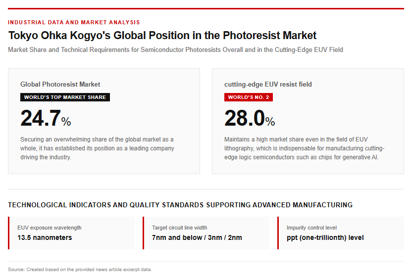
Tokyo Ohka Kogyo is an industry-leading company holding the world’s top global market share of 24.7 percent in semiconductor photoresists. Particularly in the field of EUV resists, which are essential for manufacturing cutting-edge logic such as chips for generative AI, the company holds a 28 percent share, ranking second in the world. The company’s strength lies in its comprehensive product lineup that accommodates customers’ diverse manufacturing nodes, ranging from older-generation i-line and KrF resists to state-of-the-art ArF immersion and EUV resists. Please refer to the figure below for the competitiveness and share composition in the photoresist market.
Custom technology that optimizes chemical formulations to suit the differing manufacturing processes of each semiconductor manufacturer, combined with the strong trust built through years of joint development with global foundries, forms a formidable barrier (switching cost) that deters new entrants. Together with high-purity technology that eliminates impurities to the absolute limit, this solidifies their position at the top of the global market.
Supply Chain Resilience and Future Outlook for Advanced Semiconductor Demand
Expansion of the Global Production Base Based on the Medium-Term Management Plan
Tokyo Ohka Kogyo has set the establishment of a robust supply chain as a primary goal in its medium-term management plan, the “TOK Medium-Term Plan 2027.” The newly completed new manufacturing building at the Koriyama Plant (an investment of approximately 23 billion yen) serves as a core investment of this initiative, but the company’s production base expansion strategy extends beyond Japan. In June 2026, the company commenced operations at a new plant for the “Aso Plant Aso Kumamoto Site” in Kumamoto Prefecture, and in September 2026, it also completed a new manufacturing building at the Pyeongtaek Plant of its South Korean subsidiary. Furthermore, it is promoting the full-scale operation of production bases to boost supply capacity in overseas markets. By simultaneously scaling up advanced resist production capacity across multiple domestic locations (such as Koriyama and Aso) and key overseas semiconductor manufacturing hubs, the company has established a global multi-site supply system. Through this, it is building a framework to reliably meet the rapidly growing demand from global semiconductor manufacturers such as TSMC, Samsung Electronics, and Intel.
Expansion of the Advanced Logic and AI Semiconductor Market and Key Points to Watch
In the future semiconductor market, driven by the evolution of generative AI, advanced electronic control for automotive applications, and the spread of communications, demands for advanced logic semiconductors and high-bandwidth memory (HBM) will further increase. Tokyo Ohka Kogyo has set ambitious long-term growth targets for 2030, aiming for sales of 350 billion yen (a 54.2 percent increase compared to the forecast for the fiscal year ending December 2025) and EBITDA (earnings before interest, taxes, depreciation, and amortization) of 77 billion yen (a 57.5 percent increase on the same basis). The market’s focus is on addressing the generational shift to new materials, such as metal oxide resists (MOR) accompanying the introduction of ultra-fine processes beyond the 2-nanometer node and high-numerical-aperture (High-NA) EUV lithography systems, which will gain full momentum moving forward. Across the industry as a whole, investment competition among major domestic chemical companies is intensifying, with Sumitomo Chemical announcing the construction of a new technology building at its Osaka Works that consolidates development, evaluation, and production processes, aiming for completion by the end of fiscal 2027. In the photoresist sector, where Japanese companies account for approximately 90% of the global market share, how Tokyo Ohka Kogyo will lead the industry through technological innovation and supply capacity will be a key point to watch in the future.
Reference page
- [Tokyo Ohka Kogyo Co., Ltd. News Release] https://www.tok.co.jp/news/2026
[#Semiconductor #Photoresist #TokyoOhkaKogyo #EUV #SmartFactory #MaterialTechnology]


コメント