
A research group consisting of Taiyo Nippon Sanso, Tokyo University of Agriculture and Technology, and Novel Crystal Technology has successfully formed gallium oxide films on a 6-inch wafer using the HVPE method for the first time in the world. Behind this achievement is a national project aimed at lowering the cost of next-generation power semiconductors and improving the energy efficiency of industrial equipment, including EVs.
- Key Points and Development Background of Successful 6-Inch Wafer Film Deposition
- Physical properties surpassing existing power semiconductors (SiC and GaN)
- Development of High-Precision Film Deposition Technology and Single-Wafer / Batch Equipment
- Crystal growth methods (EFG, VB, and DG methods) and cost reduction efforts
- Contribution to a Decarbonized Society and Next-Generation EVs and Industrial Equipment
- Global Market Forecasts Toward the 2030s and Key Points to Watch
Key Points and Development Background of Successful 6-Inch Wafer Film Deposition
Taiyo Nippon Sanso Corporation, Tokyo University of Agriculture and Technology, Novel Crystal Technology, Inc., and NEDO (New Energy and Industrial Technology Development Organization) announced on March 1, 2022, that they have succeeded for the first time in the world in forming a gallium oxide ($\beta$-Ga2O3) thin film on a 6-inch (150 mm) wafer using the halide vapor phase epitaxy (HVPE) method. Gallium oxide has been attracting attention as a new material for realizing high-breakdown-voltage and low-loss power devices, but conventional epitaxial deposition equipment using the HVPE method has been limited to small-diameter 2-inch and 4-inch (100 mm) single-wafer systems, and increasing the diameter to reduce device manufacturing costs has been considered the biggest challenge. In this development, 6-inch film formation on a test wafer (sapphire substrate) was demonstrated, and by adopting a proprietary source nozzle structure and optimizing film formation conditions, excellent uniformity with a film thickness distribution of within ±10% across the wafer surface was achieved. The following figure shows an overview of the developed film deposition equipment and deposition substrate.
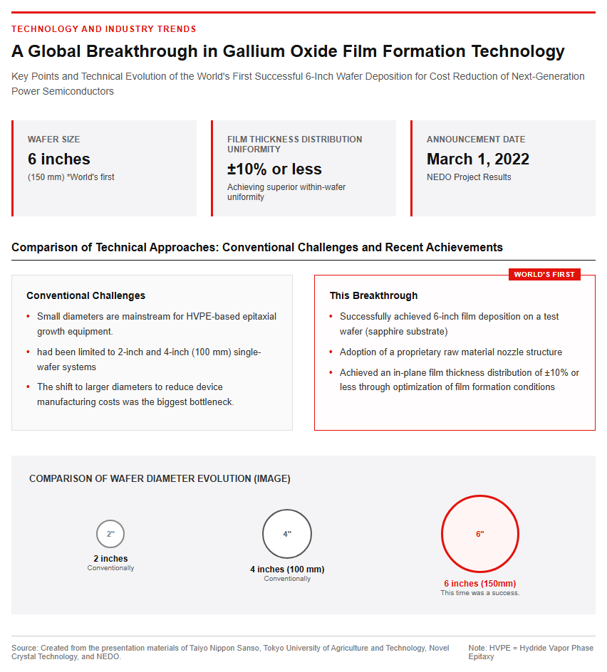
The establishment of this technology has built an important platform for the future development of batch-type, large-diameter mass-production equipment.
Physical properties surpassing existing power semiconductors (SiC and GaN)
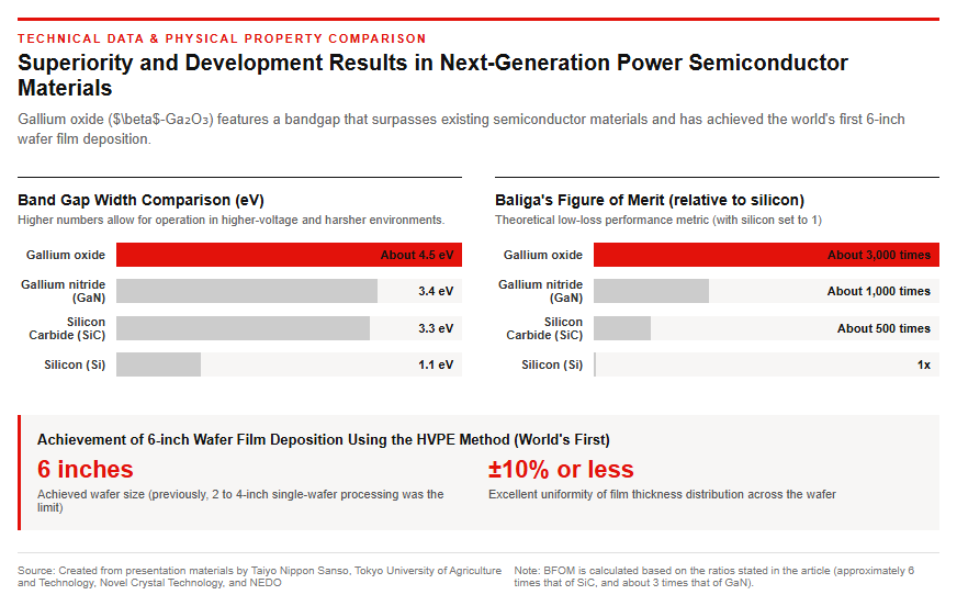
The reason why gallium oxide ($\beta\text{-Ga}_2\text{O}_3$) is attracting attention as a leading candidate for next-generation power semiconductors lies in its overwhelming physical properties. In terms of the bandgap width, which serves as a performance indicator for semiconductors, conventional silicon (Si) is 1.1 eV, whereas gallium oxide possesses a remarkably wide ultra-wide bandgap of approximately 4.5 eV. This figure surpasses even the 3.3 eV of silicon carbide (SiC) and the 3.4 eV of gallium nitride (GaN), which are currently seeing widespread adoption. When compared using the Baliga Figure of Merit (BFOM), which indicates the theoretical low-loss performance of power devices, gallium oxide boasts outstanding theoretical performance: approximately 3,000 times that of silicon, about 6 times that of SiC, and about 3 times that of GaN. Because it possesses high dielectric breakdown strength, it enables the manufacturing of diodes (SBDs) and transistors (FETs) that minimize power loss to the absolute limit even in high-voltage environments. Furthermore, unlike SiC and GaN, it has a major advantage in that bulk single crystals can be produced at high speeds and in large diameters via melt growth (a method of pulling single crystals directly from the melt), theoretically enabling a low-cost substrate supply comparable to that of silicon.
Challenges and Approaches Toward Mass Production of Gallium Oxide Substrates and Epitaxial Growth
Development of High-Precision Film Deposition Technology and Single-Wafer / Batch Equipment
The HVPE method is a crystal growth technique that uses metal chloride gas (such as GaCl) as a raw material, featuring the ability to achieve high-speed growth and high-purity film formation. As part of NEDO’s “Strategic Energy Conservation Technology Innovation Program,” Taiyo Nippon Sanso has been advancing the development of an external supply technology to stably supply metal chlorides from outside the reactor. By successfully starting up the 6-inch single-wafer HVPE system and demonstrating film formation, hardware design technology compatible with large-diameter substrates has been established. The following image shows an overview of the film formation process and measurement data.
Moving forward, we will work to further improve the quality of epitaxial film formation technology using not only sapphire substrates but also 6-inch gallium oxide single-crystal wafers, while continuously evaluating crystal defects in the films and verifying their electrical properties. Furthermore, the introduction of inspection techniques such as non-destructive, high-speed 3D defect imaging using phase-contrast microscopes will enable in-process quality control and prompt feedback to crystal growth conditions. The company aims to commercialize mass-production equipment by fiscal 2024 and enter the device manufacturing line.
Crystal growth methods (EFG, VB, and DG methods) and cost reduction efforts
Various crystal growth technologies are being researched to enable low-cost mass production of gallium oxide substrates. The EFG (Edge-defined Film-fed Growth) method, which is currently in practical use, has the challenge of easily generating processing loss because circular wafers are cut from plate-like crystals. In contrast, the Vertical Bridgman (VB) method solidifies crystals within a cylindrical crucible, making it possible to obtain high-quality crystals while suppressing processing loss, and it has also succeeded in producing 6-inch single crystals. Furthermore, innovative processes that fundamentally revolutionize raw material costs are being developed, such as the DG (Drop-fed Growth) method, which does not use expensive iridium crucibles that account for about 60% of manufacturing costs, and the OCCC method promoted by a startup originating from Tohoku University. On the substrate supply front, Novel Crystal Technology, Inc. has presented a clear roadmap—starting sample shipments of 150 mm (6-inch) substrates in March 2026, sample shipments of 150 mm epi-wafers in 2027, and full-scale mass production in 2029—accelerating the transition from the prototyping stage to the industrial mass-production phase.
The Impact of Gallium Oxide on the Industrial Sector and Future Market Forecasts
Contribution to a Decarbonized Society and Next-Generation EVs and Industrial Equipment
The practical application and widespread adoption of gallium oxide power devices will have a tremendous impact on decarbonization and energy conservation across society as a whole. Because they can dramatically reduce power loss in power conversion equipment that handles high voltages and large currents, they are expected to be widely utilized in applications such as electric vehicle (EV) drive inverters and rapid chargers, main converters for railway rolling stock, industrial motor control inverters, and power conditioners for residential solar power generation systems. Particularly in next-generation EVs, the miniaturization of inverters and improved power efficiency will directly contribute to extended cruising ranges and lighter vehicle bodies. According to estimates by the Ministry of Economy, Trade and Industry (METI) and NEDO, the power consumption reduction achieved by applying gallium oxide film formation processes and compatible devices is projected to reach approximately 210,000 kiloliters per year in crude oil equivalent in Japan by 2030. In addition, they are expected to play a core role in reducing power losses in power supplies for rapidly growing AI data centers and in renewable energy transmission and distribution grids.
Global Market Forecasts Toward the 2030s and Key Points to Watch
Gallium oxide is projected to achieve extremely high growth rates in its future market outlook. According to a survey by Fuji Keizai Co., Ltd., the market for gallium oxide epiwafers manufactured using the HVPE method is expected to reach approximately 59.0 billion yen by fiscal 2030, driven primarily by expanding demand for Schottky barrier diodes (SBDs) and field-effect transistors (FETs). Furthermore, while the overall global market for power semiconductors is projected to double to 7.3495 trillion yen by 2035, the gallium oxide power semiconductor market is also estimated to expand significantly from 14.9 billion yen to a scale of 150 billion yen. In terms of intellectual property, Japanese companies have driven the early technologies, but recent patent filing trends indicate a shift toward a Japan-China duopoly on a global scale due to the rise of China. The greatest points of focus moving forward will be the progress in manufacturing cost reductions—from the scheduled sample supply of 150 mm epiwafers in 2027 to full-scale mass production in 2029—as well as the transition to larger 200 mm (8-inch) diameters anticipated for 2035. Whether Japan-originated technology can secure the global standard will be a major key to success.
Reference Page
- [NEDO News Release] https://www.nedo.go.jp/news/press/AA5_101520.html
- [Novel Crystal Technology, Inc. Press Release] https://www.novelcrystal.co.jp/press-release/
[#GalliumOxide #PowerSemiconductors #HVPE #SemiconductorTechnology #EnergyConservation #ElectricVehicles #NextGenTech]


コメント