On June 24, 2026, Qualcomm, a major U.S. semiconductor company, announced a new memory technology for data centers, called “High Bandwidth Compute (HBC).” This technology, which achieves an overwhelming power efficiency of six times that of existing HBMs, has the potential to break through the serious bottleneck in AI inference—the ‘memory wall’—and transform the very structure of data centers.
- Key Points of the Announcement and Roadmap Released
- Challenging the ‘memory wall’ that causes stagnation in AI processing
- A new architecture combining 3D stacking and LPDDR
- Outstanding power efficiency and effective memory bandwidth
- The Arrival and Optimization of the Era of Agentic AI
- Market Outlook and Partnerships After 2026
Key Points of the Announcement and Roadmap Released
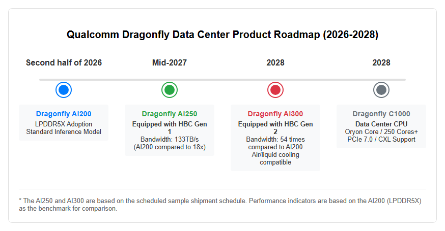
On June 24, 2026, Qualcomm unveiled a comprehensive roadmap announcing its full-scale entry into the data center market at its investor briefing “Investor Day” held in New York. The core technology announced is our proprietary near-memory computing architecture, “High Bandwidth Compute (HBC).” This technology is designed to physically bring AI computing units and memory as close as possible, minimizing power consumption associated with data movement. The company has shown ambitious plans to apply its advanced low-power computing expertise in smartphone chips to data centers, aiming to expand sales in this segment to $15 billion by 2029. As a specific product lineup, we plan to ship commercial samples of the inference accelerator “Dragonfly AI250” equipped with the first-generation HBC (HBC Gen 1) in mid-2027. Furthermore, in 2028, the company plans to launch the significantly enhanced second-generation (HBC Gen 2) “AI300” and the specially designed CPU “Dragonfly C1000,” aiming to reshape the dominant power structure in the AI infrastructure market. The following diagram shows the deployment timing of Qualcomm’s data center products.
Challenging the ‘memory wall’ that causes stagnation in AI processing
Currently, the most serious challenge in the global AI development field is the phenomenon known as the “Memory Wall.” This refers to a bottleneck state where, despite the increased computational speed of computing units (GPUs and CPUs), data transfer speeds from memory cannot keep up, resulting in computational resources not being effectively utilized. When running massive AI like large language models (LLMs), computing units often end up in a “waiting” state, consuming power while waiting for data to arrive. The current mainstream HBM (High Bandwidth Memory) offers high bandwidth but also has the drawback of being costly and requiring very high power consumption. Qualcomm’s HBC has redefined the very layout of computation and memory to resolve the fundamental bottlenecks associated with data movement. By shortening and streamlining data transport paths, they have succeeded in dramatically reducing energy losses when performing the same processes. This technology enables low-cost, low-latency real-time responses even as AI models continue to grow.
Innovation and Outstanding Performance Indicators of HBC Technology
A new architecture combining 3D stacking and LPDDR
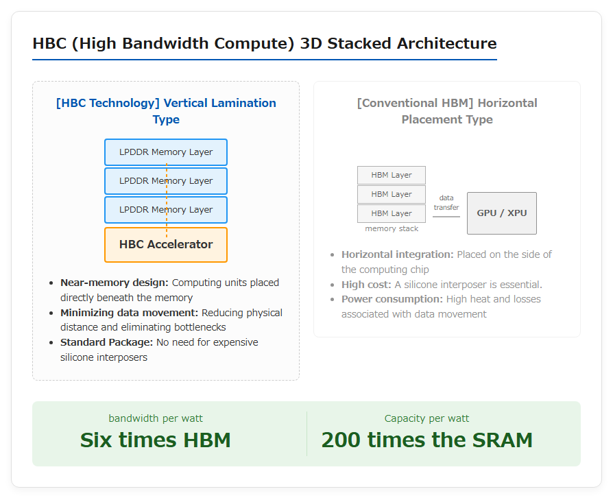
The technical core of HBC lies in the introduction of “3D laminated silicon technology” using the Through-Silicon Electrode (TSV) process. Unlike conventional HBMs that are placed on the sides of the computing chip, HBCs adopt a structure where computing units such as accelerators are stacked directly beneath the memory stack. In this structure, the storage medium adopted is “LPDDR memory,” which originally evolved for mobile devices. LPDDR features extremely low power consumption, easy stacking, and superior cost performance compared to HBM. By combining this outdated technology with a cutting-edge 3D integrated packaging process, Qualcomm has eliminated the need for expensive silicon interposers while ensuring outstanding data transfer capabilities. This enables the deployment of multiple HBC stacks within a single device using standard packaging, significantly reducing the total cost of ownership (TCO) of the system. Please refer to the diagram below to illustrate how HBC’s physical laminated structure works.
Outstanding power efficiency and effective memory bandwidth
The greatest advantage of HBC is its outstanding power efficiency. According to Qualcomm’s official announcement, HBC delivers up to six times the performance of competing HBM technologies in “bandwidth per watt” at the card level. This means moving six times more data with the same power consumption, making it an extremely attractive proposition for data center operators facing operational challenges in power costs. Furthermore, in terms of memory capacity per watt at the rack level, it has achieved a dramatic improvement of 200 times that of SRAM. As a specific performance figure, the “AI250” scheduled for release in 2027 achieves industry-leading effective memory bandwidth of 133TB/s per card, which is an 18-fold improvement compared to the previous LPDDR5X-equipped model (AI200). The next-generation “AI300” will see further improvements, with bandwidth expected to be increased up to 54 times that of the AI200. Such extreme performance improvements make it possible to stably operate AI inference at scales that were previously impossible even in air-cooled or simple liquid-cooled environments.
Future Developments and AI Infrastructure Transformation
The Arrival and Optimization of the Era of Agentic AI
Qualcomm is particularly focused on the next-generation form of AI called “Agentic AI” in the development of HBC technology. Agentic AI refers to AI agents that go beyond simply answering questions, autonomously making decisions and performing complex tasks. In an era where AI is becoming more widespread, massive token processing required for always-on operation will be required, and power efficiency and real-time responsiveness will be decisive factors in business success. HBC is optimized for these agent-driven workloads, designed to maintain high throughput while reducing power consumption per token. The company is not only providing hardware but also actively strengthening its software ecosystem, including acquiring AI software company Modular for approximately $3.9 billion. By providing everything from chips to compilers and development tools in an integrated package, we aim to compete with NVIDIA’s robust CUDA moat and establish leadership in the inference accelerator market.
Market Outlook and Partnerships After 2026
The memory market in 2026 is expected to continue the HBM-led supercycle, with the market size approaching $1 trillion. While SK Hynix and Samsung Electronics fiercely compete for dominance in the HBM market, Qualcomm is aiming to enter the market with its unique strategy of “replacing HBM with LPDDR.” Proving the effectiveness of this strategy lies in strong partnerships with major hyperscalers. Meta has officially confirmed that it will adopt Qualcomm’s “Dragonfly C1000” CPUs in its next-generation server fleet. Additionally, Microsoft Azure has expressed its intention to deploy HBC chips. The support from these two giants is evidence that Qualcomm’s technology has practical potential to complement or partially replace NVIDIA’s GPUs in real-world commercial environments. As the competitive axis of AI data centers shifts from “computing power” to “economics per token and power efficiency,” HBC has the potential to be a game-changer in the semiconductor market in the late 2020s.
[#半導体 #AIインフラ #Qualcomm #HBC #HBM #データセンター #省エネ #次世代技術]
コメント