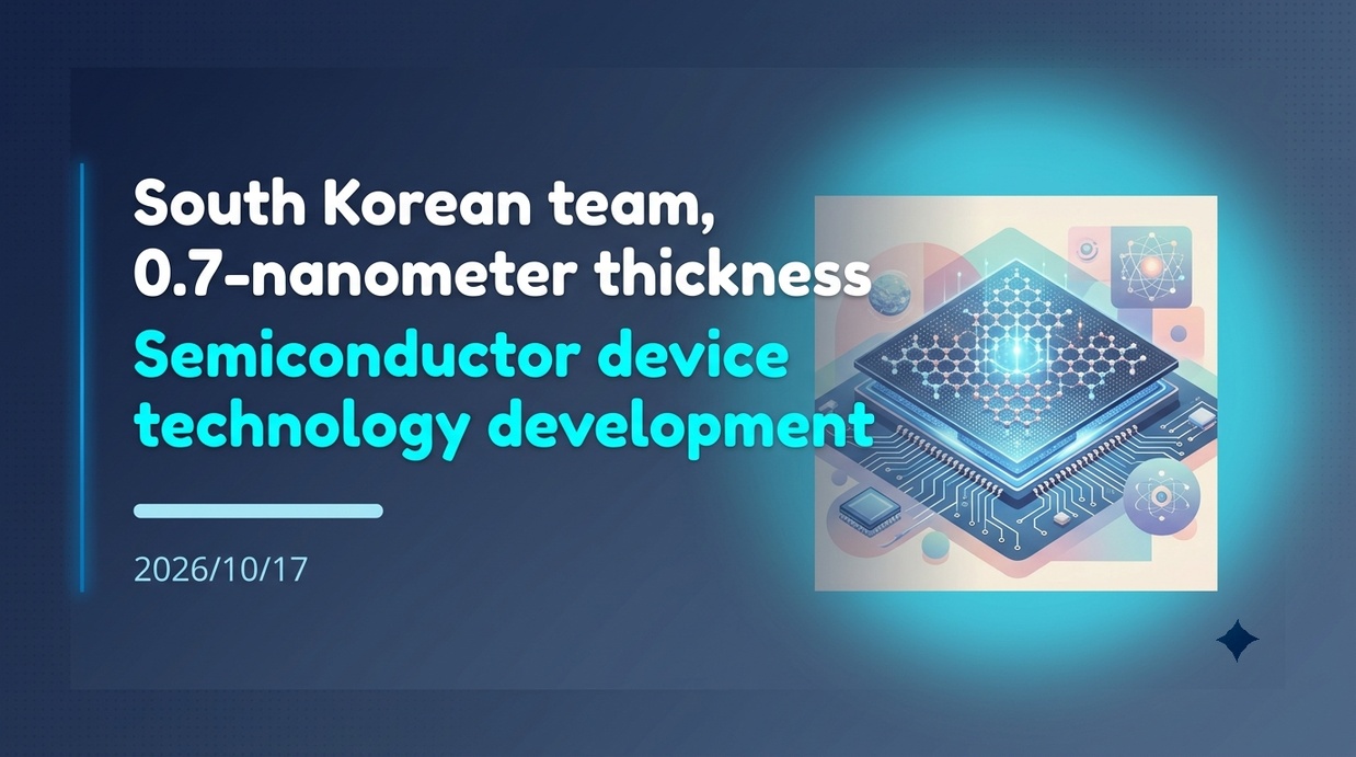
A research team at South Korea’s Institute for Basic Science (IBS) has developed a 0.7-nanometer-class two-dimensional semiconductor device using atomic substitution technology, which was published in the international academic journal Science. As conventional silicon miniaturization processes face physical limits, it is attracting global attention as a new approach to integrally form circuit elements on a single thin film without undergoing complex stacking processes.
- Key Points of the Event and the Impact of the Research Announcement
- The Mechanism of Atomic Substitution Technology That Alters Physical Properties on a Single Thin Film
- Operating efficiency approaching theoretical limits and overwhelming reduction of the energy barrier
- Vertical Stacking of Complementary Inverters Opening Up 3D Integrated Circuits
- The Limits of Silicon and a Comparison of Trends with Global Competitors Such as IBM
- Challenges Toward Mass Production and Expected Future Social Significance
Key Points of the Event and the Impact of the Research Announcement
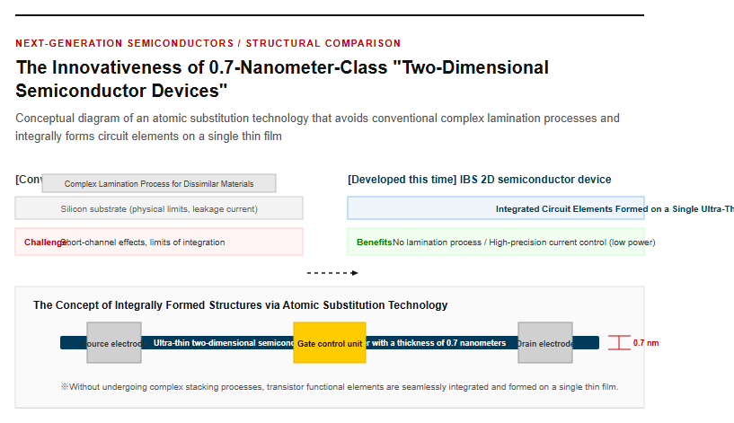
On October 16, 2026, South Korea’s Ministry of Science and ICT announced that a research team led by Director Cho Moon-ho (POSTECH professor) of the Van der Waals Quantum Materials Research Center at the Institute for Basic Science (IBS) has developed a fabrication technology for next-generation semiconductor devices with a thickness of 0.7 nanometers. The research results were published on the same day in the world’s most prestigious U.S. science journal, Science. Following the 3D integration technology “NanoStack” announced by U.S.-based IBM in June 2026, this technological development marks the world’s second-ever achievement in realizing a 0.7-nanometer-class device. In conventional silicon semiconductors, the short-channel effect—where leakage current occurs with the ultra-miniaturization of line width and film thickness—has become severe, and physical limits to improving integration density have been pointed out. In contrast, two-dimensional semiconductors are expected to be the leading material for realizing next-generation ultra-miniature, low-power chips because they can control current with high precision despite their atomic-layer-level ultra-thin structure. This research has sent shockwaves through the semiconductor industry by demonstrating an innovative method that avoids the conventional manufacturing process of complexly stacking multiple different materials, instead integrally forming all necessary elements for a transistor within a single thin film. The following figure shows the structure of the two-dimensional semiconductor device prototyped using this technology.
The Mechanism of Atomic Substitution Technology That Alters Physical Properties on a Single Thin Film
The core method developed by the research team is called “modular transistor fabrication technology.” In conventional two-dimensional semiconductor development, it was necessary to stack different materials one by one—a semiconductor layer through which current flows, an insulating film layer that blocks and controls the current, and a metal electrode layer that inputs and outputs the current. This resulted in non-uniform contact between different materials and an increase in contact resistance, which have been major obstacles to practical application. To solve this problem, instead of stacking materials, the research team devised a method to selectively replace the atoms making up the base two-dimensional semiconductor. The substrate used was tungsten diselenide (WSe₂), a p-type semiconductor with a structure in which a tungsten atomic layer is sandwiched from above and below by selenium atomic layers. While keeping the central tungsten atoms intact, only the surrounding selenium atoms were precisely replaced by adjusting the pressure and temperature of the reaction gas. Specifically, the following replacements are carried out.
- Replacing Selenium with Oxygen: Forming Insulating Tungsten Oxide
- Replacing Selenium with Sulfur: Formation of Tungsten Disulfide, an n-Type Semiconductor
- Replacing selenium with tellurium: Forming tungsten ditelluride (an electrode contact layer), a metalloid with high electrical conductivity
By combining manufacturing masks with a technology that precisely halts the diffusion of chemical reactions at the 0.7-nanometer atomic layer level, we have successfully and selectively imparted the required electrical properties to targeted locations on a flat surface.
Overwhelming electrical performance and device structure that surpass conventional technology
Operating efficiency approaching theoretical limits and overwhelming reduction of the energy barrier
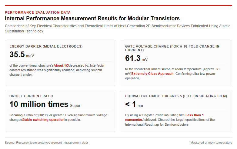
A modular transistor fabricated by integrating a semiconductor, an insulating film, and a semimetal electrode junction layer within a single thin film demonstrated overwhelming electrical characteristics that far surpass conventional direct metal bonding methods. The energy barrier that acts as an obstruction when charges move from the metal electrode to the semiconductor dropped to 35.5 millielectronvolts (meV), achieving an extremely low value of approximately one-third that of the conventional structure with directly attached electrodes. This significantly reduces contact resistance at the interface, enabling extremely smooth current control. In addition, the gate voltage change required to vary the current tenfold was recorded at 61.3 millivolts (mV). This is a figure extremely close to the theoretical minimum limit achievable by conventional silicon transistors at room temperature (approximately 60 mV), strongly supporting the realization of ultra-low power consumption operation. Furthermore, the ratio between the on and off states of the current is secured at 10 million (10^7) times or more, allowing stable switching even with slight voltage changes. The equivalent oxide thickness (EOT), which is a performance index of the tungsten oxide insulating film, also achieved less than 1 nanometer, clearing the target specifications for state-of-the-art ultrafine devices set forth by the International Roadmap for Devices and Systems. An overview of the internal performance measurement results of the device can be found in the following image.
Vertical Stacking of Complementary Inverters Opening Up 3D Integrated Circuits
The true value of this research lies in its demonstration of flexibility that extends beyond the formation of a single transistor element to actual digital logic circuits and advanced integrated circuits. The research team adopted a structure in which p-type and n-type transistors, fabricated using atomic substitution technology, are vertically stacked to construct a complementary inverter circuit (CMOS inverter), which forms the absolute basis of digital circuits. This vertically stacked inverter exhibited favorable switching behavior, accurately inverting and outputting input electrical signals even under a low-voltage drive environment of just 1 volt (V). While conventional planar silicon circuits have reached their limits in reducing the footprint (occupied area) as density increases, a three-dimensional integration approach that vertically stacks two-dimensional semiconductor sheets serves as a key technology for dramatically increasing computational density without increasing the mounting area. Requiring no complex bonding processes for heterogeneous substrates and capable of three-dimensionally constructing logic circuits with atomic-layer-level control, this method holds the potential to bring about a revolution in the design of future ultra-high-density CPUs and AI-dedicated accelerators.
The Approaching Footsteps of the Next-Generation Semiconductor Competition and Future Prospects
The Limits of Silicon and a Comparison of Trends with Global Competitors Such as IBM
In the semiconductor industry, Taiwan’s TSMC and South Korea’s Samsung Electronics are currently locked in a race to commercialize 2-nanometer processes, but yield management in manufacturing and massive capital expenditures have become major hurdles. For instance, Samsung Electronics’ yield for its first-generation 2-nanometer process stands at only around 55%, falling short of the 60% threshold considered the line of profitability, illustrating that silicon scaling is facing severe technical and economic bottlenecks. Against this backdrop, the development of “sub-1-nanometer” technologies—measuring less than 1 nanometer—is intensifying as an approach to break through these physical limits. The 0.7-nanometer “NanoStack” process announced by U.S.-based IBM in June 2026 was a research breakthrough that vertically stacked silicon-based transistors, boasting a 50% performance increase or a 70% improvement in power efficiency compared to the 2-nanometer node. In contrast, the technology recently announced by South Korea’s IBS uses a novel material known as a “two-dimensional semiconductor” rather than following an extension of silicon, achieving 0.7-nanometer-class device operation. This marks the world’s second-ever demonstration of a sub-1nm device. Blending materials science with nanofabrication technology, this paradigm shift is emerging as a promising option to extend Moore’s Law for the next decade and beyond.
Challenges Toward Mass Production and Expected Future Social Significance
While the 0.7-nanometer-class two-dimensional semiconductor technology has achieved historic results as a piece of basic research, there are still challenges to be overcome toward its commercialization and mass production in foundries. The biggest concern is whether the atomic substitution reaction can be uniformly scaled from a laboratory-scale small thin film to an entire 300-millimeter (12-inch) industrial wafer. There is an urgent need to establish process technology that maintains the yield of atomic substitution over large areas and minimizes crystal defects and impurity contamination to the utmost limit. Moving forward, the research team plans to expand its application to transition metal dichalcogenide materials other than tungsten diselenide (such as molybdenum disulfide), while aiming for wafer-scale film formation and the implementation of high-capacity three-dimensional integrated circuits. If established, this technology could dramatically improve the power efficiency of AI data centers, where explosive power consumption has become a social issue, as well as edge AI terminals and ultra-compact IoT devices. In the semiconductor industry as a national strategic technology, future trends in industry-academia collaboration will be closely watched to see whether this technology, derived from basic science, can transition to the commercialization phase.
Reference Page
- [Paper Published in Science (IBS Research on 2D Semiconductor Modular Transistors)] https://www.doi.org/10.1038/s41467-026-68320-8
【#Semiconductors #2DSemiconductors #Nanotechnology #QuantumMaterials #UltrafineProcessing #NextGenerationTechnology】


コメント