Global semiconductor giants such as NVIDIA and Samsung Electronics are rapidly strengthening their partnerships with Japanese companies that support their manufacturing base, focusing on high-performance materials, precision manufacturing equipment, and physical AI-related technologies. Behind this is the upgrading of manufacturing lines driven by the explosive expansion of AI demand, as well as a strong reliance on indispensable Japanese technologies across the entire supply chain.
- Nvidia and Samsung’s Latest Trends and Focus on Japanese Technology
- Japan’s Major Material Shares That Quietly Control Global Semiconductor Production
- The Rise of Physical AI and Smart Factory Innovation
- Silicon Island Kyushu’s Aim for a Development and Manufacturing Ecosystem
- Foreign Exchange Act Amendments and Legal and Security Measures for Technology Leakage Prevention
- Next-Generation Supply Chain Transformation and Future Key Focus Areas
Nvidia and Samsung’s Latest Trends and Focus on Japanese Technology
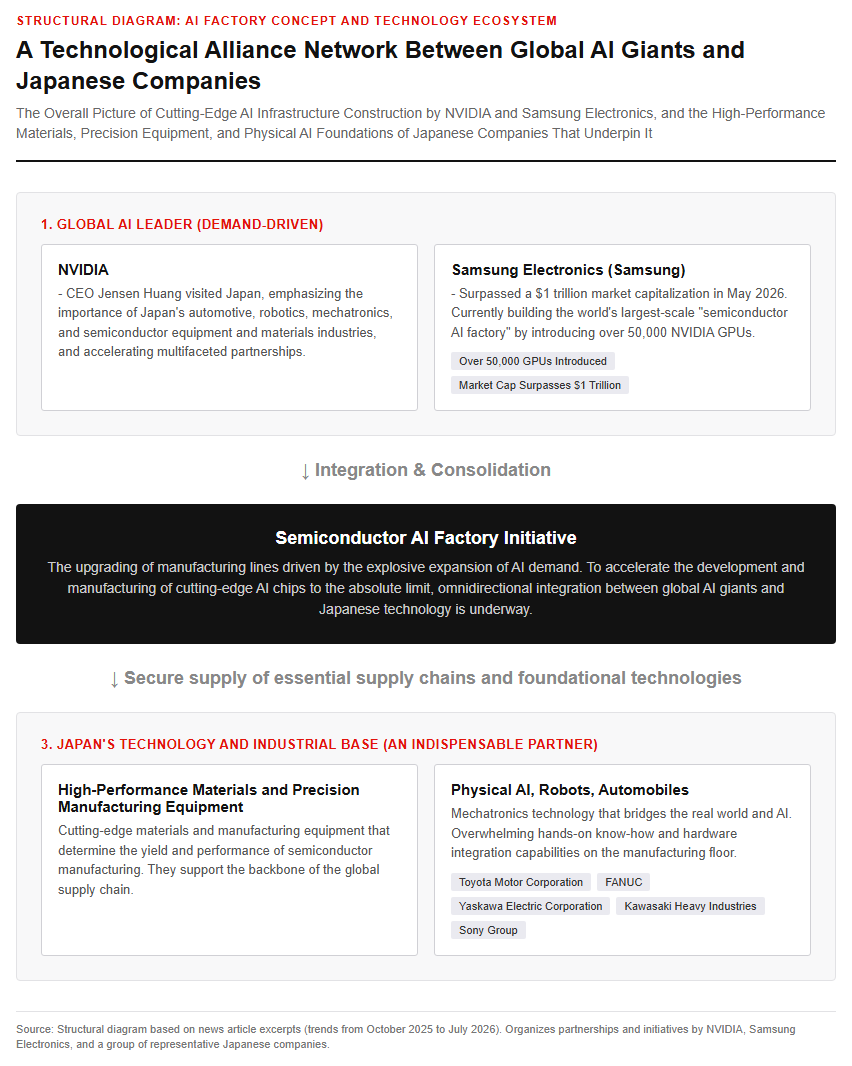
Entering 2026, alongside the global expansion of the artificial intelligence market, NVIDIA and Samsung Electronics—which lead the global semiconductor industry—have been turning their keen attention to the foundational technologies of Japanese companies one after another. In July 2026, NVIDIA CEO Jensen Huang visited Japan and emphasized the importance of Japan’s strengths in automobiles, industrial robots, mechatronics, and the semiconductor manufacturing equipment and materials industries. The company successively announced multifaceted partnerships with representative Japanese manufacturing enterprises such as Toyota Motor, FANUC, Yaskawa Electric, Kawasaki Heavy Industries, and Sony Group. Meanwhile, Samsung Electronics, which surpassed a market capitalization of $1 trillion in May 2026, also announced a strategic partnership with NVIDIA at the Asia-Pacific Economic Cooperation meeting held in October 2025. Samsung is advancing plans to introduce over 50,000 NVIDIA graphics processing units to build the world’s largest-scale “Semiconductor AI Factory.” The realization of this grandiose AI factory initiative is said to require omnidirectional cooperation with Japan’s advanced semiconductor material and equipment manufacturers. As global AI giants accelerate the development and manufacturing of cutting-edge AI chips, Japan’s precision technologies and on-the-ground know-how supporting them from the ground up are once again being re-evaluated by the world. The figure below shows the overall picture of the AI Factory initiative.
Japan’s Major Material Shares That Quietly Control Global Semiconductor Production
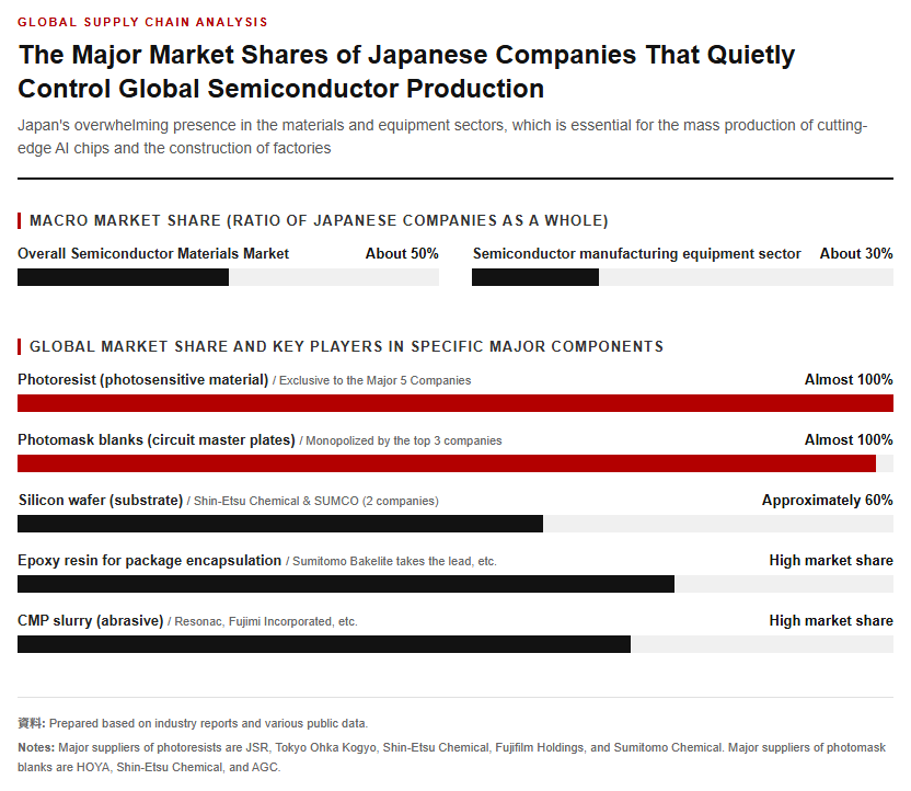
Behind the flashy news surrounding finished chip design and manufacturing processes, the actual semiconductor production lines are supported by the fields of materials and manufacturing equipment, where Japanese companies boast overwhelming strength. Japanese companies account for approximately 50% of the global semiconductor materials market and maintain roughly a 30% share in the manufacturing equipment sector. In silicon wafers—the base substrates for semiconductors—just two Japanese companies, world leader Shin-Etsu Chemical and second-place SUMCO, hold about 60% of the global market share. Global foundries such as Taiwan’s TSMC, America’s Intel, and South Korea’s Samsung Electronics find themselves in a position where they have no choice but to rely on Japanese companies for the supply of high-quality wafers. Furthermore, in photoresists—the photosensitive materials used to print circuit patterns—five major companies (JSR, Tokyo Ohka Kogyo, Shin-Etsu Chemical, Fujifilm Holdings, and Sumitomo Chemical) monopolize nearly 100% of the global market. In photomask blanks, which serve as the original circuit plates, three companies—HOYA, Shin-Etsu Chemical, and AGC—nearly monopolize the global market, while Resonac Holdings and Fujimi Incorporated hold strong market shares in CMP slurries, which are used as abrasives. Including Sumitomo Bakelite, the top player in epoxy resins for package encapsulation, the industry is structured in such a way that the mass production of cutting-edge semiconductors is utterly impossible without the high-quality components provided by Japanese companies.
The Impact of Next-Generation Manufacturing Innovation and Kyushu’s “Physical AI Land”
The Rise of Physical AI and Smart Factory Innovation
While generative AI focuses on on-screen information processing, “Physical AI,” which automates physical tasks in the real world where gravity, friction, and inertia exist, is attracting attention as a next-generation innovation on manufacturing floors. AI factories utilizing “Omniverse,” a digital twin platform promoted by NVIDIA and Samsung Electronics, are advanced intelligent factories that collect data in real time from all processes ranging from design to manufacturing, inspection, and quality control, allowing AI itself to analyze, predict, and control them. Here, initiatives are underway to maximize production efficiency by running simulations on production lines reproduced in a virtual space and coordinating autonomous robots and humanoids. Furthermore, through research on intelligent base stations utilizing AI-RAN (a next-generation mobile communication technology) and the introduction of virtual metrology technology for real-time in-process measurement, a balance between improving yields and reducing power consumption is being achieved. In implementing such Physical AI, attempts to convert high-quality manufacturing know-how and tacit knowledge—typified by Japan’s “Toyota Way” cultivated on-site over many years—into digital assets have become essential. By fusing AI technology with Japanese precision hardware technology, the productivity of the manufacturing industry is being elevated to an unprecedented new dimension. The following figure illustrates the integrated system of Physical AI and robot control.
Silicon Island Kyushu’s Aim for a Development and Manufacturing Ecosystem
The Kyushu region, which is receiving global attention as a major hub for the semiconductor industry, is transforming from its function as a “Silicon Island” into a “Physical AI Island,” a global cluster for physical AI. Following the operational launch of TSMC-backed JASM’s Kumamoto Plant 1 at the end of 2024, its second plant, scheduled to begin operations in 2028, plans to produce semi-advanced processors that will also be used for AI data centers. The Kyushu region originally has the profile of a “Car Island” with a concentration of factories belonging to Toyota Motor, Nissan Motor, and others, and Kitakyushu City is home to Yaskawa Electric, a global industrial robot company. Furthermore, core industries are closely clustered within a compact area, including the shipbuilding industry centered around Nagasaki Prefecture and renewable energy facilities represented by the Kitakyushu Hibikinada Offshore Wind Farm. In July 2026, centered around Kumamoto Prefecture and Mitsui Fudosan, the “Kumamoto Science Park” initiative progressed, with the establishment of the “Physical AI and Semiconductor Technology Center (PASTEC)” as its core. With the successive entry of overseas companies, such as the establishment of an R&D base by U.S.-based Amkor Technology in Fukuoka Prefecture, a major ecosystem spanning from research and development to design, manufacturing, and demonstration testing is being formed.
Strengthening Economic Security and the Outlook for a Sustainable Semiconductor Industry
Foreign Exchange Act Amendments and Legal and Security Measures for Technology Leakage Prevention
As the importance of cutting-edge semiconductors and robotics technologies increases dramatically, the Japanese government is rapidly advancing the protection of foundational technologies and the strengthening of management systems from the perspective of economic security. Through revisions to the Foreign Exchange and Foreign Trade Act (Foreign Exchange Act) promoted by the Ministry of Finance, the screening system for investments that could undermine national security has been significantly enhanced while promoting sound inward direct investment. Specifically, requirements for risk mitigation measures in prior notifications have been made mandatory, tracking of indirect acquisitions of domestic companies by foreign investors has been established, and monitoring systems for investors under the control of non-residents have been strengthened. To ensure a cross-ministerial screening framework, the Japan Foreign Investment Committee (JFIC) was established to safeguard domestic companies holding critical technologies. Concurrently, the National Police Agency’s Foreign Affairs and Economic Security Division and other bodies are stepping up outreach activities toward corporations and research institutions. They are providing guidance on the designated management of confidential information and the establishment of internal security rules to prevent the unintended leakage of sensitive information via cyberattacks, espionage, or joint ventures. To maintain technological superiority and indispensability, it has become essential to operate the dual wheels of promoting open collaborative research and implementing robust measures to prevent technology leakage in a well-balanced manner.
Next-Generation Supply Chain Transformation and Future Key Focus Areas
The global semiconductor industry is about to enter a period of twin transitions, driven by the acceleration of production processes through AI and adaptation to environmental and ESG regulations—typified by the Carbon Border Adjustment Mechanism (CBAM) and the Corporate Sustainability Due Diligence Directive (CSDDD) being advanced by the European Union. In academic research as well, the establishment of a “Safe and Sustainable by Design (SSbD)” architecture, which incorporates safety margins and sustainability from the product design stage, is being advocated. This calls for a mechanism that links real-time data obtained from in-line sensors and virtual metrology with digital material passports to prove the environmental impact across the entire product lifecycle. Moving forward, beyond simply riding the wave of cutting-edge investments by NVIDIA and Samsung Electronics, establishing a standardization infrastructure that enables the interoperability of data on materials, equipment, and manufacturing processes—areas where Japanese companies hold strengths—in a digital space will be emphasized. As national projects centered around Rapidus and industry-academia-government collaborations in Kyushu move into full swing from 2026 onward, the presence that Japanese companies continue to project as indispensable key players in the global AI and semiconductor supply chains will significantly influence the trajectory of global economic growth and security.
Reference page
- 【Scoping Review of AI, Metrology, and ESG in the Semiconductor Sector】[suspicious link removed]
- [Act for Partial Amendment of the Foreign Exchange and Foreign Trade Act (Ministry of Finance)][suspicious link removed]
- [Toward the Prevention of Technology Leakage (National Police Agency)] [suspicious link removed]
[#Semiconductors #NVIDIA #SamsungElectronics #PhysicalAI #SiliconIslandKyushu #ForeignExchangeAct #EconomicSecurity]


コメント