
Mitsubishi Chemical Group has finalized plans to begin sample shipments of 6-inch (150mm) gallium nitride (GaN) substrates during fiscal year 2026 (ending March 2027). As the expansion of AI data centers and electric vehicles (EVs) creates an urgent demand for enhanced power conversion efficiency, global expectations are mounting for GaN as a foundational material for next-generation power semiconductors.
- Overview of 6-Inch GaN Substrate Sample Shipments Targeted for FY2026
- Cost Reduction Breakdown Driven by Low-Pressure Ammonothermal Technology (SCAAT-LP)
- Physical Limits of Silicon and the Strategic Advantages of GaN over SiC
- Rapid Demand Growth Triggered by AI Data Centers and EV High-Voltage Systems
- TSMC’s Market Exit and the Upstream Material Strength of Japanese Firms
- Future Outlook and Key Factors for Mass Production and Commercial Adoption
Overview of 6-Inch GaN Substrate Sample Shipments Targeted for FY2026
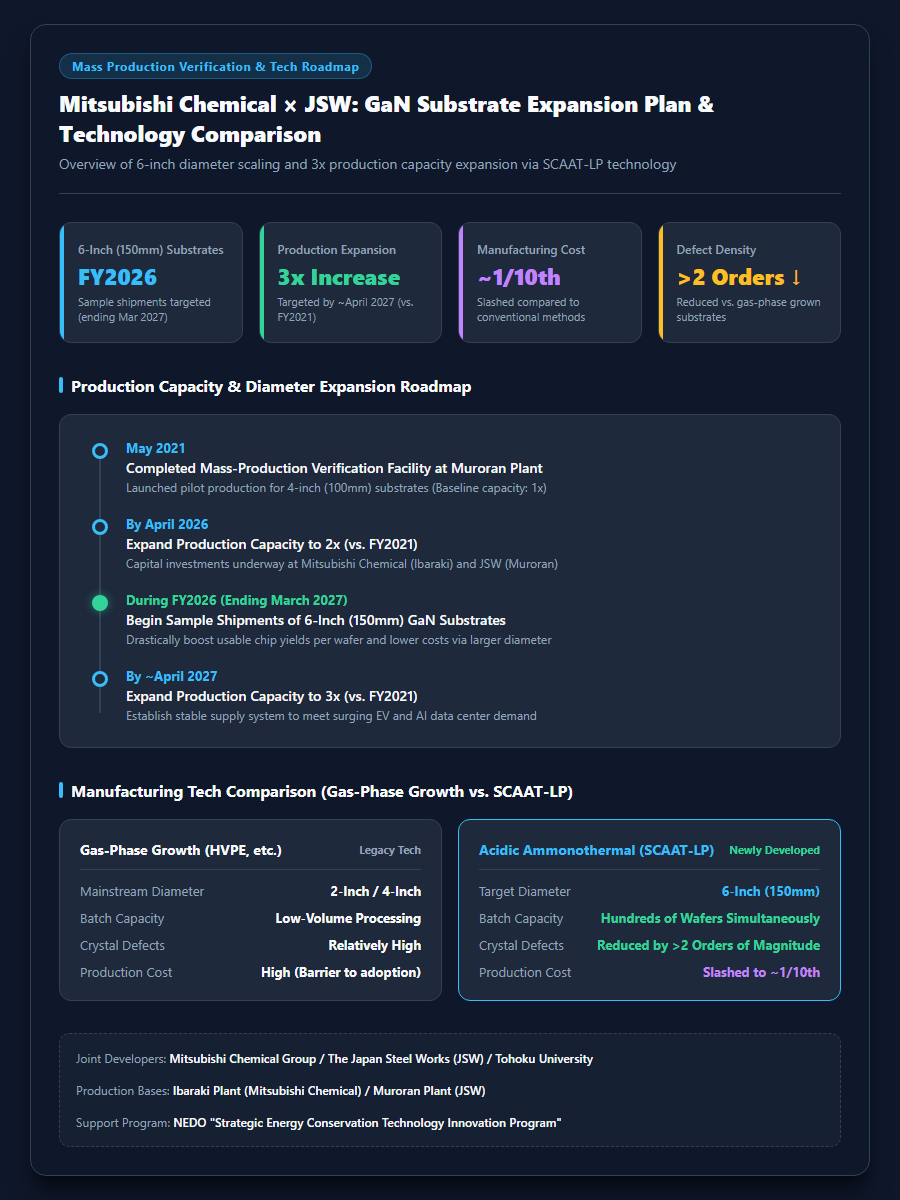
Mitsubishi Chemical Group announced its policy to begin sampling 6-inch (150mm) gallium nitride (GaN) substrates for next-generation power semiconductors during fiscal year 2026 (ending March 2027). While power semiconductor substrates have traditionally centered on 2-inch and 4-inch (100mm) sizes, moving to larger diameters drastically increases the yield of usable chips per wafer, enabling substantial reductions in manufacturing costs. Mitsubishi Chemical has been jointly developing GaN substrates with The Japan Steel Works (JSW). In May 2021, the partners completed a mass-production verification facility at JSW’s Muroran Plant and launched pilot production of 4-inch substrates. Furthermore, both companies are advancing plans to double their production capacity relative to FY2021 by April 2026, and to triple it by around April 2027. Capital investments are underway at Mitsubishi Chemical’s Ibaraki plant and JSW’s Muroran Plant to establish a stable supply system for large-diameter GaN substrates. The following figure illustrates the concept of GaN crystal manufacturing at the mass-production pilot plant.
This initiative has also been selected for the “Strategic Energy Conservation Technology Innovation Program” by the New Energy and Industrial Technology Development Organization (NEDO), accelerating technology development toward the commercial adoption of next-generation power semiconductors through industry-academia-government collaboration.
Cost Reduction Breakdown Driven by Low-Pressure Ammonothermal Technology (SCAAT-LP)
The primary barrier to the widespread adoption of GaN substrates has been the high cost stemming from the sheer difficulty of crystal growth. Mitsubishi Chemical, JSW, and Tohoku University jointly developed “SCAAT-LP” technology, an evolution of the acidic ammonothermal method “SCAAT” that grows single crystals in high-temperature, high-pressure ammonia while reducing the required operating pressure. Compared with conventional gas-phase growth methods such as hydride vapor phase epitaxy (HVPE), SCAAT-LP utilizes large pressure vessels to simultaneously grow hundreds of high-quality GaN crystals in a single batch. This process yields large single crystals with exceptional quality and uniformity, reducing crystal defect density by more than two orders of magnitude compared to traditional gas-phase grown substrates. Furthermore, establishing this manufacturing process is projected to slash production costs to approximately one-tenth of conventional methods. Building an infrastructure capable of supplying high-voltage, high-efficiency power devices in large volumes at low cost represents a major technical breakthrough for the broader power electronics market.
The Role and Market Demand for GaN in Next-Generation Power Electronics
Physical Limits of Silicon and the Strategic Advantages of GaN over SiC
Silicon (Si) has dominated power electronics for decades, but it is approaching its physical limits regarding power conversion efficiency and thermal management in high-voltage, high-frequency environments. Consequently, wide-bandgap semiconductors such as silicon carbide (SiC) and gallium nitride (GaN) have emerged as primary alternatives. While SiC excels in high-voltage, high-temperature environments and is already commercialized in EV main traction inverters, GaN possesses distinct physical characteristics: superior electron mobility and ultra-fast switching speeds. Because GaN dramatically minimizes switching power losses, it enables power supply circuits to achieve miniaturization, weight reduction, and higher efficiency simultaneously. While conventional lateral GaN-on-silicon (GaN-on-Si) devices have been confined to low-to-medium voltage applications, vertical GaN devices (GaN-on-GaN) built on the single-crystal GaN substrates slated for shipment can withstand high voltages ranging from 700V to over 1,700V. This gives vertical GaN the potential to challenge and outpace SiC in high-voltage markets.
Rapid Demand Growth Triggered by AI Data Centers and EV High-Voltage Systems
Rapid expansion in AI data centers and technological breakthroughs in electric vehicles are driving an unprecedented surge in demand for GaN substrates. Graphics processing unit (GPU) servers used for training and running generative AI models consume immense electrical power, making data center energy efficiency and thermal cooling reduction urgent priorities. Applying vertical GaN devices to 800V high-voltage direct current (HVDC) power distribution systems is expected to cut power losses by roughly 50% while reducing power supply unit volume by 50%. The following diagram outlines the power conversion architecture in AI data centers and EVs.
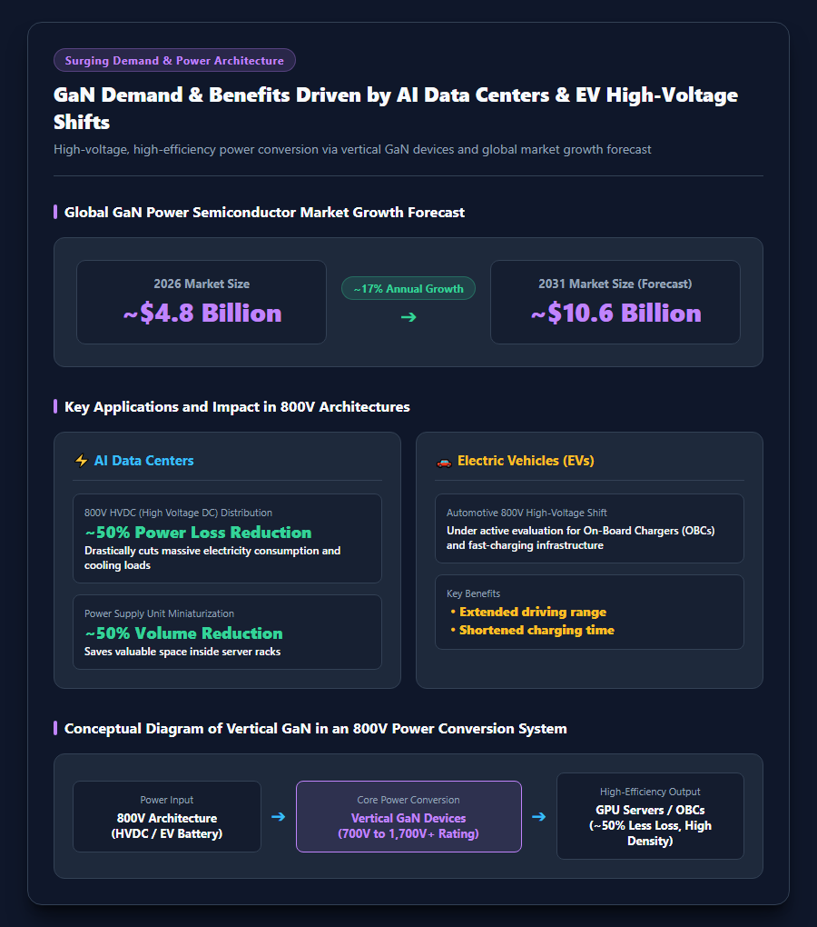
Similarly, the automotive sector is accelerating its transition to 800V architectures to extend driving range and shorten charging times, spurring rapid evaluation of GaN adoption in on-board chargers (OBCs) and fast-charging infrastructure. With the global GaN market projected to grow from approximately \$4.8 billion in 2026 to \$10.6 billion by 2031 at a compound annual growth rate (CAGR) of 17%, the market urgently awaits a reliable supply of practical, large-diameter substrates.
Global Semiconductor Competition and Japan’s Substrate Oligopoly Strategy
TSMC’s Market Exit and the Upstream Material Strength of Japanese Firms
Major structural shifts are reshaping the global GaN semiconductor landscape. TSMC, the world’s largest foundry, decided to completely exit the GaN manufacturing business by July 2027, driven in part by low-price competition from Chinese suppliers. In response, Japanese companies are stepping in to fill the vacuum; for instance, Rohm acquired process technology licenses from TSMC to transition and scale up 8-inch wafer mass production at its own fabs. Amid intense competition in device manufacturing, Japanese suppliers—including Mitsubishi Chemical Group, Sumitomo Chemical, and Sumitomo Electric Industries—maintain a dominant global oligopoly in single-crystal GaN substrates, the critical core of vertical GaN. Mirroring Japan’s enduring strength in semiconductor equipment, this “upstream victory strategy” of controlling raw materials and substrate supply chains is yielding tangible strategic results.
Future Outlook and Key Factors for Mass Production and Commercial Adoption
The rollout of 6-inch GaN substrate sample shipments by Mitsubishi Chemical Group is poised to be a game-changer for the power semiconductor industry. Following sample evaluation by device manufacturers, the industry expects a transition toward 8-inch scaling between 2027 and 2028, alongside full-scale integration into automotive and industrial systems. Meanwhile, intellectual property competition is intensifying, as evidenced by frequent patent litigation between European, US, and Chinese firms. Securing market trust will require combining high-quality substrates with a robust patent portfolio. As TSMC’s complete withdrawal in 2027 converges with Japanese manufacturers launching 8-inch production and delivering a steady supply of high-quality 6-inch substrates, all eyes are on whether Japanese players can successfully secure leadership in the global next-generation power semiconductor race.
Reference Pages
- [Gallium Nitride Substrates | Product Information | Mitsubishi Chemical Corporation] https://www.m-chemical.co.jp/products/departments/mcc/nes/product/1200584_9018.html
[#GalliumNitride #GaNSubstrates #MitsubishiChemical #NextGenPowerSemiconductors #ElectricVehicles #DataCenters #JapanSteelWorks]


コメント