NVIDIA has announced a comprehensive plan to significantly expand the manufacturing capacity of its supply chain in order to meet the rapid growth in demand for AI infrastructure. This backdrop is driven by the current reality where not only is there a shortage in the supply of GPUs alone, but the entire back-end process—including substrate packaging, advanced packaging, semiconductor testing, and optical communication components—has become a bottleneck in the construction of AI factories.
- Major expansion plan aimed at eliminating bottlenecks across the entire manufacturing process
- Package substrate production capacity to be increased 2.5-fold over the next 3 years
- Enhancement of Advanced Packaging and Testing Capabilities and Upfront Investments
- Dramatic Reduction in Construction Time Through the Modular “DSX POD”
- Co-packaged optics (CPO) and a 15-fold increase in optical engine production
- Roadmap for Mass Production Launch and Key Points to Watch
Major expansion plan aimed at eliminating bottlenecks across the entire manufacturing process
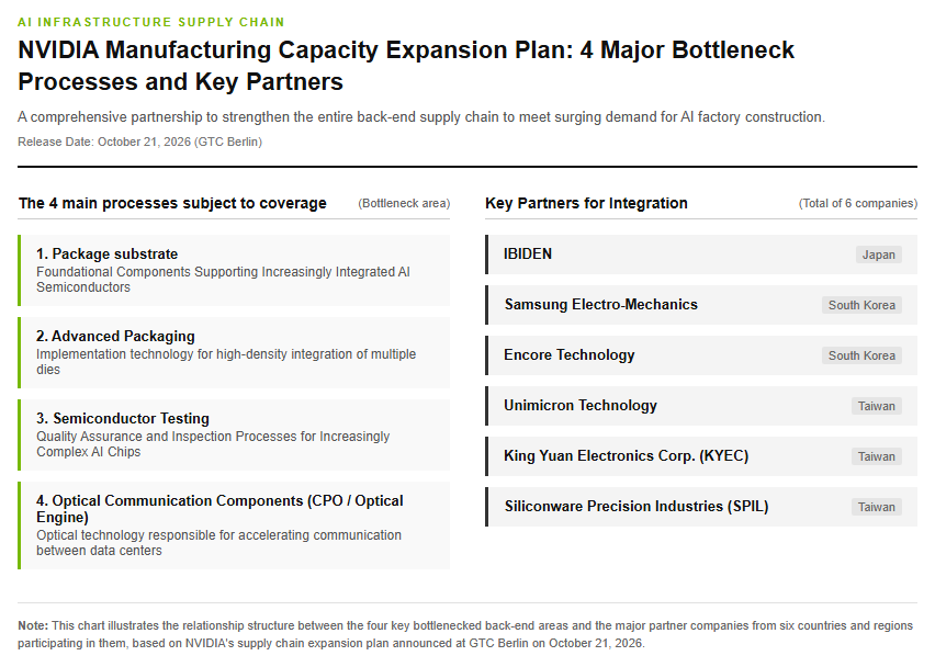
On October 21, 2026, at GTC Berlin held in Berlin, Germany, NVIDIA announced plans to expand its manufacturing capacity in collaboration with six supply chain partners to meet the surging demand for accelerated computing and AI factories. NVIDIA CEO Jensen Huang stated, “Demand is extraordinary, and production capacity is the bottleneck,” demonstrating his determination to accelerate infrastructure deployment. The scope of this expansion goes beyond mere GPU chip manufacturing, covering four key processes: package substrates, advanced packaging, semiconductor testing, and optical engines used in co-packaged optics (CPO). The partnering companies include Japan’s Ibiden, South Korea’s Samsung Electro-Mechanics and Amkor Technology, as well as Taiwan’s Unimicron Technology, King Yuan Electronics (KYEC), and Siliconware Precision Industries (SPIL). While traditional semiconductor supply chains have tended to focus on circuit formation on silicon wafers, for modern AI semiconductors, the supply capacity of back-end processes and peripheral components has become the primary constraint determining system shipment volumes. This announcement aims to simultaneously reinforce vulnerabilities across these multifaceted supply networks, thereby enhancing the redundancy and resilience of global manufacturing capabilities. The following figure illustrates the relationship between the key partners and the targeted processes.
Package substrate production capacity to be increased 2.5-fold over the next 3 years
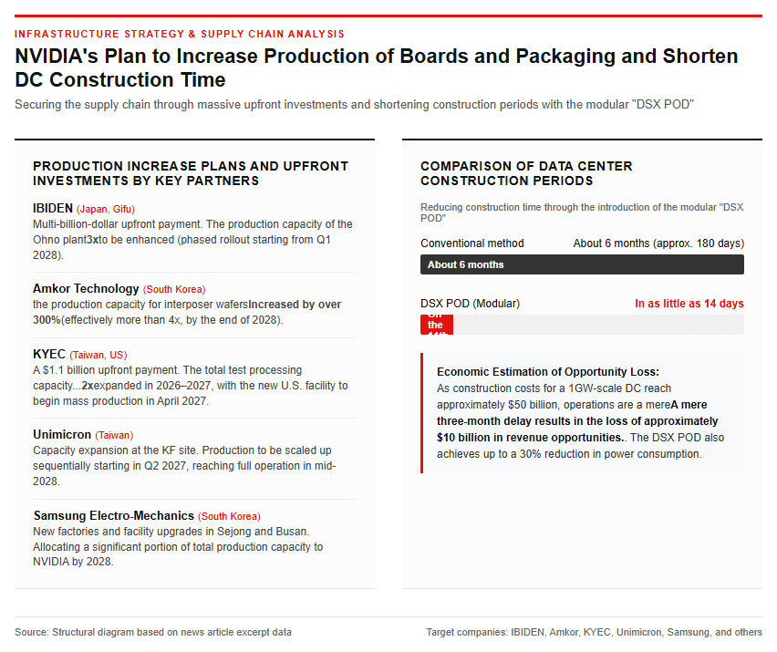
In the field of package substrates, which are essential for AI semiconductor implementation, a policy was outlined to expand the total production capacity of substrates for NVIDIA products by 2.5 times over the next three years through strengthened partnerships with three companies: Ibiden, Samsung Electro-Mechanics, and Unimicron. For Japan’s Ibiden, multi-billion-dollar prepayments will be made to secure production capacity at the Ohno Plant in Gifu Prefecture. The Ohno Plant aims to triple its conventional production capacity, with the launch of the additional capacity scheduled to begin phased implementation in the first quarter of 2028. Additionally, South Korea’s Samsung Electro-Mechanics, which has newly joined the supply chain, is advancing the development of new factories in Sejong and Busan as well as the improvement of existing facilities, with plans to allocate a substantial portion of its total annual package substrate production capacity to NVIDIA by 2028. Furthermore, Taiwan’s Unimicron is also proceeding with capacity expansion at its KF site, with plans to sequentially start increased production from the second quarter of 2027 and reach full capacity by mid-2028. These substrate production increase plans are linked to each company’s existing factories and new investments, aiming to establish a long-term and stable substrate supply system.
Strengthening Backend Processes and Data Center Construction Innovation
Enhancement of Advanced Packaging and Testing Capabilities and Upfront Investments
In parallel with the expansion of package substrates, the enhancement of advanced packaging and testing systems that enable high-density semiconductor integration is also being vigorously promoted. Through a collaboration with South Korea’s Amkor Technology, plans have been established to increase interposer wafer production capacity by more than 300% by the end of 2028. This indicates that the increase will exceed three times the current production capacity, which means the actual supply capacity will effectively reach over four times the current level. Furthermore, in the semiconductor testing process, total throughput is projected to double between 2026 and 2027 through the expansion of facilities in the United States, Taiwan, and Singapore. Specifically, an advance payment of $1.1 billion will be provided to Taiwan’s KYEC to secure production capacity, supporting the setup of new testing facilities and equipment in the United States. This facility aims to start mass production in April 2027. Additionally, mass production at the expanded testing facility in Singapore is scheduled to begin in February 2027. NVIDIA’s approach of taking the initiative to provide large-scale advance funding to mitigate the capital investment risks of its partner companies can be described as a strategic move to lock in the supply chain and secure guaranteed production capacity.
Dramatic Reduction in Construction Time Through the Modular “DSX POD”
To improve the deployment speed of AI infrastructure, NVIDIA has unveiled its next-generation modular data center solution, “DSX POD.” DSX POD is a container-standardized, box-type facility where servers, wiring, closed-loop liquid cooling systems, and other components are pre-assembled and verified at a factory before being transported to the site. On sites equipped with the necessary infrastructure, installation work can be completed in a short time, making it possible to drastically shorten the on-site construction period of data centers from the conventional approximately 6 months to as little as 14 days. CEO Jensen Huang emphasized the importance of construction speed, presenting an estimate that with the construction cost of a 1-gigawatt (GW) scale data center reaching approximately $50 billion, a mere 3-month delay in operation would result in the loss of about $10 billion in revenue opportunities. Additionally, the DSX POD is based on the next-generation AI platform “Vera Rubin” and is equipped with closed-loop liquid cooling that significantly reduces water usage, as well as software called “DSX MaxLPS” that cuts power consumption by up to 30%. This innovative modular approach is planned to be rolled out globally starting in early 2027 in collaboration with major server OEMs such as Dell, HPE, and Foxconn. A reference diagram illustrating the conceptual structure is placed within the text.
Future Outlook for Next-Generation Connectivity Technologies and the AI Supply Chain
Co-packaged optics (CPO) and a 15-fold increase in optical engine production
To curb data transmission latency and power consumption in large-scale AI computing, NVIDIA is also accelerating the adoption of optical communication technology. Through a partnership with Taiwan’s SPIL (Siliconware Precision Industries), the company will dramatically expand domestic manufacturing capacity in Taiwan for optical engines used in co-packaged optics (CPO). The plan aims to scale production capacity to 15 times previous levels by mid-2027, and double it once more by the end of 2028. CPO is a technology that tightly integrates optical engines and switching chips within a single package, achieving dramatic reductions in transmission power and higher speeds compared to conventional plug-in optical modules. As the number of parameters in AI models explodes, chip-to-chip and rack-to-rack data interconnectivity has become a critical factor dictating system performance. Consequently, the early establishment of CPO technology and the securing of mass production capacity are directly tied to performance enhancements in next-generation supercomputers.
Roadmap for Mass Production Launch and Key Points to Watch
This announcement makes it clear that NVIDIA has expanded its role from a semiconductor circuit designer to an infrastructure architect for entire AI factories. However, the announced production increase plans do not immediately translate to an increased supply of AI systems. The production increase schedules vary across manufacturing processes, with multiple milestones spread out over time: the operation of the Singapore testing facility in February 2027, the mass production at KYEC’s US facility in April, a 15-fold increase in optical engines by SPIL in mid-2027, and the startup of Ibiden’s Ono plant in the first quarter of 2028. Because a certain time lag occurs from factory construction and equipment installation to the actual stabilization of yields and full operation, it is necessary to carefully assess whether each process proceeds according to plan. In addition, running parallel to the expansion of manufacturing supply capacity, another key focus moving forward will be whether the securing of power supplies, preparation of land and buildings, and progress in financing on the customer side align properly. Only when the processes across the entire supply chain ramp up in sync will the full operation of next-generation AI factories become a reality.
Reference page
- https://nvidianews.nvidia.com/news/nvidia-and-supply-chain-partners-expand-capacity-to-accelerate-ai-infrastructure-buildout
【#NVIDIA #AISemiconductors #SupplyChain #Ibiden #Amkor #DSX_POD #CPO】
コメント