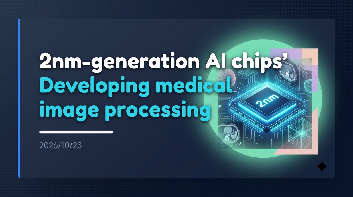
Five parties, including the Leading-edge Semiconductor Technology Center (LSTC) and Hokkaido University, have announced the joint development of a high-speed, low-power medical image processing system utilizing 2nm-generation semiconductors specialized for inference. The background to this is the goal of overcoming the barriers of processing delays and high power consumption in current GPUs—which accompany the shift toward large-capacity data in next-generation medical devices—thereby realizing real-time diagnosis and surgical support in medical settings.
- The Launch of the Domestic 2nm Project and the Overall Picture of the Five-Party Collaboration
- Inference-Optimized 2nm Chips and the Two-Stage Development Approach
- 3 Real-Time Support Systems Transforming Medical Settings
- The Significance of Problem-Solving and Energy Conservation in Clinical Settings
- Development Structure and Validation of Utility at Hokkaido University Hospital
- Hurdles to Practical Application and Future Points of Focus
The Launch of the Domestic 2nm Project and the Overall Picture of the Five-Party Collaboration
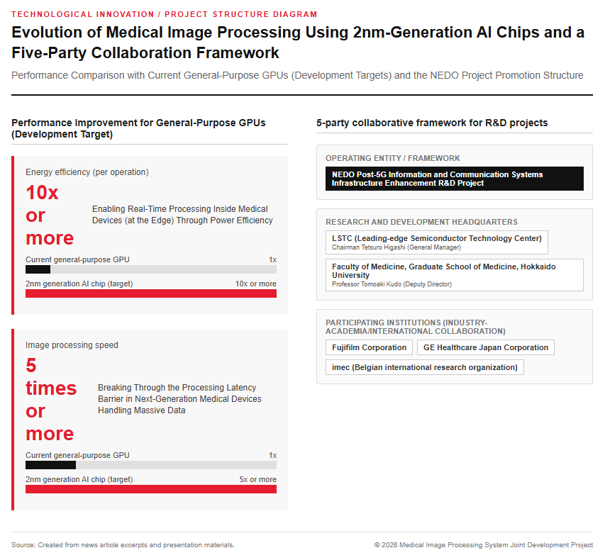
On October 20, 2026, five organizations—the Leading-edge Semiconductor Technology Center (LSTC), Hokkaido University, FUJIFILM Corporation, GE Healthcare Japan Corporation, and the Belgian international research organization imec—announced that a new research and development project has been selected under the New Energy and Industrial Technology Development Organization (NEDO)’s “Project for Enhanced Infrastructural Technology Development for Post-5G Information Communication Systems / Development of Advanced Semiconductor Manufacturing Technology.” The project is titled “Research and Development of High-Speed, Low-Power Medical Image Processing Systems Utilizing Inference-Optimized 2nm-Generation Semiconductors,” with Tetsuro Higashi, Chairman of LSTC, serving as the Project Director, and Yoshiaki Kudo, Professor at the Faculty of Medicine, Hokkaido University, serving as the Deputy Project Director.
The purpose of this project is to fundamentally resolve the two major bottlenecks in applying AI to the medical field—”high power consumption” and “processing latency”—by using state-of-the-art 2nm-generation semiconductors. Japanese industry, academia, and international research institutions will work together to build a high-performance inference processing infrastructure that operates directly near (at the edge) inside medical devices. As a development goal, we aim for a dramatic performance improvement, achieving over 5 times the image processing speed and over 10 times the energy efficiency per process compared to the general-purpose GPUs currently mainstream in medical settings. It is attracting attention as a pioneering project that presents social implementation use cases for cutting-edge semiconductors planned for domestic manufacturing. As shown in the figure below, the fusion of advanced semiconductors and medical equipment is showing new developments.
Inference-Optimized 2nm Chips and the Two-Stage Development Approach
AI computing processes consist of two types: “training,” which learns patterns from vast amounts of data, and “inference,” which analyzes unknown data using a trained model. In image analysis AI that functions in medical settings in coordination with diagnostic equipment and surgical instruments, the training function is unnecessary, and the processing capability for “inference”—which analyzes input images as quickly and accurately as possible—is critically important. While conventional general-purpose GPUs support a wide range of calculations, they feature many circuit areas that are unnecessary for medical inference processing, which has been a factor causing high power consumption, heat generation, and processing delays.
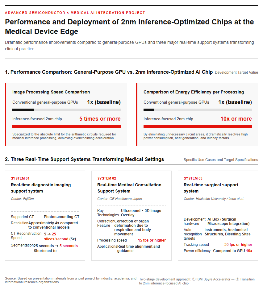
Therefore, this project will adopt a 2nm-generation AI chip specialized to the absolute limit for the arithmetic circuits required for inference processing. In the development process, a two-step approach is planned to achieve a smooth technology transition. As the first step, we will proceed with constructing and optimizing the AI model architecture on IBM’s preceding hardware, the “IBM Spyre Accelerator”. Subsequently, as the second step, the development results will be ported and deployed to the primary 2nm-generation inference-specialized AI chip.
This phased development approach makes it possible to enhance the maturity of software and algorithms in parallel with the hardware manufacturing process. Through the close co-design of advanced semiconductor processes and medical-specific AI, we aim to achieve both overwhelming processing power and ultra-energy-saving performance that were previously unattainable with conventional GPU configurations.
3 Real-Time Support Systems Transforming Medical Settings
In this research and development project, to meet specific medical needs, we will develop the following three advanced real-time support systems. First is the “Real-Time Diagnostic Imaging Support System,” spearheaded by Fujifilm. To support next-generation “photon-counting CT”—which boasts approximately four times the resolution of conventional systems and a data volume that swells by 3 to 5 times—we will develop a deep learning-based high-speed CT image reconstruction AI and an organ segmentation AI capable of identifying 1,000 types of anatomical structures across the entire circumference. We aim to achieve a 5-fold increase in the current reconstruction speed, from 5 slices per second to 25 slices per second, and to reduce the segmentation time from 25 seconds to 5 seconds.
Second, there is the “real-time medical care support system” handled by GE Healthcare Japan. This is a technology that overlays ultrasound images and 3D CT or MRI images in real time, displaying the overlaid images at a speed of 15 fps (frames per second) or higher while correcting for organ deformation caused by respiration and body movement. Third, there is the “real-time surgery support system” being developed by Hokkaido University and imec. They are developing an “AI Box” that automatically recognizes and tracks surgical instruments, anatomical structures, and bleeding sites in real time from surgical microscope footage, aiming for a tracking speed of 30 fps or higher and a power efficiency 10 times that of GPUs. Please refer to the figure below for the configuration that visualizes the on-site medical care provision system.
Social Implementation in Medical Settings and Future Outlook
The Significance of Problem-Solving and Energy Conservation in Clinical Settings
In modern advanced medical settings, the volume of image data captured is increasing dramatically due to the higher performance of modalities (diagnostic imaging equipment). Particularly with next-generation equipment represented by photon-counting CT, the amount of information obtained is so vast that current processing GPUs require significant time for reconstruction and analysis, creating situations where the equipment had to be operated with reduced resolution and performance. If processing speeds can be improved by more than five times using a 2nm-generation inference-optimized chip, high-definition diagnostic images can be outputted immediately after scanning, leading to shorter patient wait times and a significant reduction in the reading burden on physicians.
Furthermore, achieving power savings with over 10 times the energy efficiency directly contributes not only to reducing operational costs for medical institutions, but also to building a sustainable healthcare environment (GX: Green Transformation). By suppressing heat generation, it becomes possible to integrate the technology compactly directly into medical devices themselves (edge deployment), eliminating the need for large cooling equipment or external cloud servers. This makes it possible to provide advanced AI image diagnosis equivalent to that of urban core hospitals even in rural and depopulated medical facilities, free from network latency and security risks, serving as a major stepping stone toward resolving regional healthcare disparities.
Development Structure and Validation of Utility at Hokkaido University Hospital
A major strength of this project lies in its industry-academia-government international collaborative framework that covers the entire value chain, from semiconductor design to medical device development and clinical validation. LSTC, a research platform for cutting-edge semiconductor technology, will oversee the overall coordination, while imec, a world-renowned semiconductor research institute in Belgium, will provide advanced compilation technologies such as quantization and pipeline optimization. Furthermore, Fujifilm and GE Healthcare Japan, which boast world-class track records in diagnostic imaging equipment and medical IT systems, will drive commercialization development under the premise of integrating the system into actual CT scanners, PACS (picture archiving and communication systems), and image-reading workstations.
And Hokkaido University is solely responsible for verifying the clinical validity and usefulness of the developed AI algorithms and hardware. Centering on the Department of Diagnostic Imaging at the Hokkaido University Graduate School of Medicine and the Medical AI Research and Development Center at Hokkaido University Hospital, they will rigorously evaluate accuracy, safety, and operability in an environment close to actual medical settings. By going through a verification process directly linked to the university hospital’s clinical data, it accelerates the construction of practical systems that go beyond mere technological development, keeping future regulatory approval and clinical implementation in mind.
Hurdles to Practical Application and Future Points of Focus
For the social implementation of medical AI systems using cutting-edge 2nm-generation AI chips, several technical and institutional challenges must be overcome moving forward. The first hurdle is the migration of AI models from the development environment, the IBM Spyre Accelerator, to the final 2nm inference-specialized AI chip. This requires optimization processes to prevent accuracy degradation associated with heterogeneous hardware migration and to fully leverage the computing power of the hardware. Furthermore, another important factor will be aligning the timing of the establishment of mass-production systems for the 2nm process at cutting-edge foundries, such as Rapidus established in Japan, with the progress schedule of system development.
The second hurdle is the regulatory approval procedure as a medical device, which requires strict safety and reliability. For algorithms that aim to continue improving performance even after commercialization, proper implementation of regulatory compliance is essential, including the utilization of the IDATEN (Modification Plan Confirmation Procedure) system, the legal processing of training data using pseudonymized information, and ethical reviews (compliance with guidelines on life science and medical research). Steadily executing the two-step approach and enhancing clinical compatibility with medical settings toward practical application in the late 2020s will be the primary focus moving forward.
Reference page
- [NEDO Post-5G Information and Communication Systems Infrastructure Enhancement Research and Development Project] https://www.nedo.go.jp/koubo/IT3_100373.html
- 【Technology Research Association Leading-edge Semiconductor Technology Center (LSTC)】[suspicious link removed]
- [National University Corporation Hokkaido University][suspicious link removed]
- [Fujifilm Corporation News Release] [suspicious link removed]
- [GE Healthcare Japan Corporation][suspicious link removed]
- 【imec (Interuniversity Microelectronics Centre)】[suspicious link removed]
【#LSTC #2nmSemiconductors #MedicalAI #MedicalImageProcessing #NEDO #HokkaidoUniversity #Fujifilm #GEHealthcare】


コメント