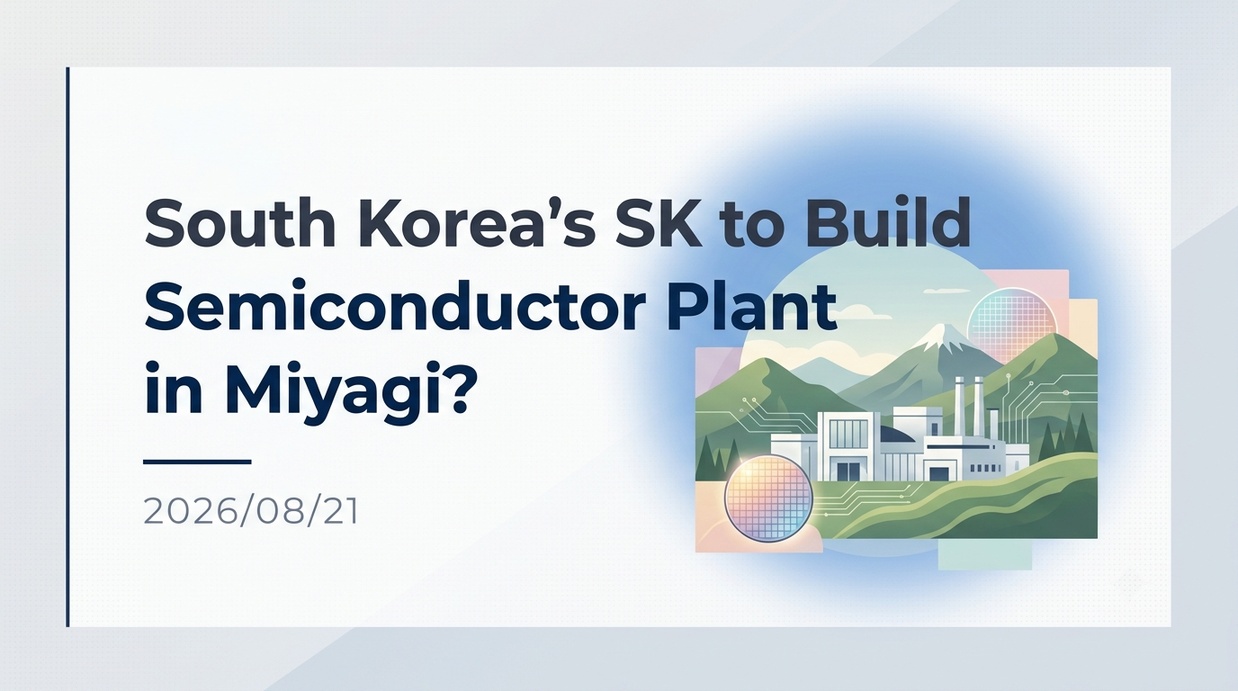
It has been revealed that South Korean semiconductor giant SK hynix is advancing plans to build a memory chip plant worth several trillion yen in Miyagi Prefecture. The move is backed by Miyagi Prefecture’s aggressive efforts to attract investment—prompted by the withdrawal of Taiwan’s PSMC—and the significant cost advantages offered by Japan’s generous subsidy programs.
- Key takeaway: Reports of SK hynix’s massive investment in Miyagi Prefecture, Japan
- Background: Miyagi Prefecture’s Efforts to Overcome the Challenge of PSMC’s Withdrawal
- Strategic Factors: Generous Japanese Government Support and Cost Advantages
- A Plan in Flux: The Path from Denying Expansion to a Policy Shift
- Geopolitical Complexities: US Pressure and the Constraints of Domestic Public Opinion in South Korea
- Future Developments: Relaunch of the Miyagi Silicon Valley Initiative and Key Points for Realization
Key takeaway: Reports of SK hynix’s massive investment in Miyagi Prefecture, Japan
On August 21, 2026, South Korean media outlets including The Hankyoreh reported that semiconductor giant SK Hynix is considering investing tens of trillions of won (several trillion yen) to build a memory semiconductor production plant in Miyagi Prefecture, located in Japan’s Tohoku region. According to reports, SK Group Chairman Chey Tae-won personally visited the proposed site in Miyagi. If realized, this would mark the company’s first large-scale production investment in Japan. Alongside Kyushu and Hokkaido, Miyagi is one of three major hubs being nurtured by the Japanese government as a semiconductor industry center. Amid ongoing global memory semiconductor shortages, SK Hynix is advancing massive cluster investments worth hundreds of trillions of won domestically in places like Yongin and Honam, and the Miyagi plant project is positioned as a preemptive move to expand overseas production capacity in parallel with these efforts.
Background: Miyagi Prefecture’s Efforts to Overcome the Challenge of PSMC’s Withdrawal
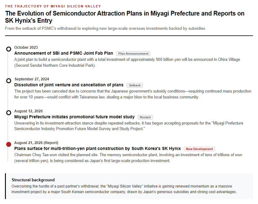
Miyagi Prefecture’s Ohira Village has faced significant challenges in its efforts to attract semiconductor manufacturers. In October 2023, SBI Holdings and major Taiwanese semiconductor foundry PSMC announced a joint plan to build a semiconductor plant with a total investment of approximately 900 billion yen. However, just about a year later on September 27, 2024, the two companies announced the dissolution of their joint venture, completely scrapping the project. The decision was driven by concerns that the Japanese government’s subsidy requirement—mandating over 10 years of continued mass production—might conflict with Taiwanese regulations. This sudden withdrawal dealt a severe blow to the local business community and regional banks in the Tohoku region, including The 77 Bank, which had high expectations for massive capital demand and business matching with local suppliers after launching semiconductor project teams and hosting large-scale seminars.
Undeterred, Miyagi Prefecture has continued its aggressive efforts to attract new investments to Ohira Village’s “Second Sendai Northern Core Industrial Park,” most recently issuing a call for proposals on August 12, 2026, for a “Miyagi Prefecture Semiconductor Industry Promotion Future Model Survey and Study.” The recent reports regarding SK Hynix’s entry signal a restart of the local community’s long-held dream to establish a semiconductor hub.
Please refer to the figure below.
The Cost Structure Attracting Massive Investment and the Ever-Shifting Business Strategy
Strategic Factors: Generous Japanese Government Support and Cost Advantages
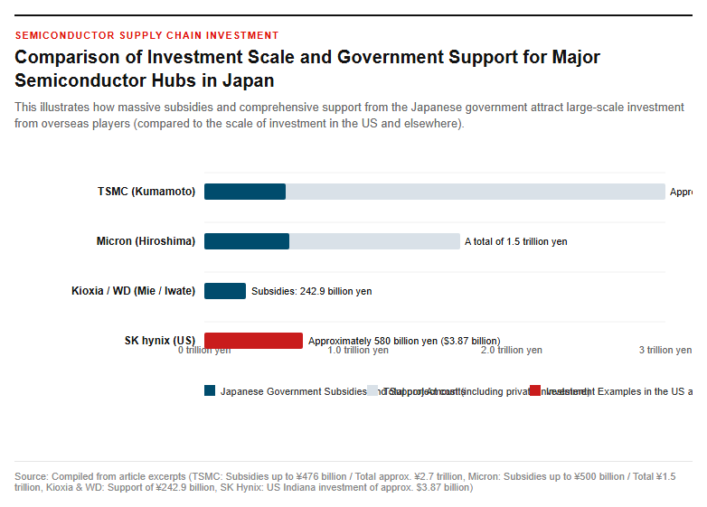
For semiconductor manufacturers, building factories in Japan is considered an extremely rational choice from a purely business perspective. According to an analysis revealed by a Samsung Electronics semiconductor division executive, building and operating a memory plant in Japan can reduce initial investment and total cost of ownership (TCO) by about half compared to South Korea. While South Korea’s government incentives tend to be insufficient and incur additional costs, Japan offers a comprehensive “full package” of support, including massive subsidies, tax breaks, infrastructure development, workforce securing assistance, and collaboration with local equipment and material suppliers. Taiwan’s TSMC has already built a plant worth approximately 2.7 trillion yen in Kumamoto Prefecture with up to 476 billion yen in subsidies, and U.S.-based Micron Technology is proceeding with a new 1.5 trillion yen next-generation HBM plant in Hiroshima Prefecture with up to 500 billion yen in government support. Furthermore, Kioxia and Western Digital are receiving a total of 242.9 billion yen in support for their plants in Yokkaichi, Mie Prefecture, and Kitakami, Iwate Prefecture. This accelerating trend of overseas competitors expanding their operations by leveraging massive Japanese government subsidies is believed to have driven SK Hynix’s decision-making.
A Plan in Flux: The Path from Denying Expansion to a Policy Shift
Discussions surrounding SK Hynix’s expansion into Japan have gone through a complex and shifting process. Although Chairman Chey Tae-won previously stated, “We are investigating whether we can produce memory in countries like Japan and the U.S.,” as of March 2026, the company officially denied rumors of building a memory plant in Japan. At the time, amid strong demands from U.S. President Donald Trump, the company had indicated its focus on building an HBM packaging plant in Indiana, U.S., investing approximately $3.87 billion (around 580 billion yen) with a target for mass production in 2028. The U.S. government had warned through industrial policies that it would impose tariffs of up to 100% on memory manufacturers failing to invest domestically, and SK Hynix showed a stance prioritizing U.S. resource allocation, such as establishing an AI-focused investment firm in the U.S. in January 2026 to scale up investments to the $10 billion level. However, the semiconductor industry is in an era where the availability of subsidies can make the impossible possible, and it is widely viewed that the Japanese government’s unprecedented support measures and, above all, the persistent global memory shortage have pulled the company’s plans back toward constructing an additional factory in Japan.
Please refer to the figure below.
Geopolitical Risks in Global Markets and Miyagi’s Future Prospects
Geopolitical Complexities: US Pressure and the Constraints of Domestic Public Opinion in South Korea
As SK hynix moves to flesh out its investment plans in Miyagi Prefecture, it still needs to overcome numerous complex barriers. The biggest risk factor is strong pressure from the US government demanding the expansion of memory production within the United States. With limited investment funds and resources, there is concern that proceeding with a massive investment in Japan could provoke wariness from the White House—which is pushing for US investment—and further complicate decisions regarding future production bases. Additionally, the semiconductor industry is a backbone of the South Korean economy, and establishing a large-scale production base in Japan, with which South Korea has a complex historical relationship, is likely to stir up concerns within South Korea about “technology leakage” and the “hollowing out of domestic industries.” Thus, despite the significant financial benefits, multiple external constraints—including harsh public opinion and political pressure in South Korea, backlash from stakeholders, and the US’s America-first industrial policy—are intricately intertwined, requiring SK hynix’s management to navigate the situation with extreme delicacy.
Future Developments: Relaunch of the Miyagi Silicon Valley Initiative and Key Points for Realization
If the plan is officially approved, it is expected to create synergistic effects with Tokyo Electron Miyagi, a major global semiconductor manufacturing equipment supplier based in Taiwa, Miyagi Prefecture. To meet the surging demand for plasma etching equipment used in AI and advanced logic applications, Tokyo Electron Miyagi is investing approximately 104.1 billion yen to build a new production facility with a total floor area of around 88,000 square meters, having held a groundbreaking ceremony in June 2025 ahead of its completion in the summer of 2027. Once operational, this is expected to eventually triple the production capacity of the Taiwa base. Furthermore, LAPIS Semiconductor Miyagi, a ROHM Group company that mass-produces semiconductors for automotive and IoT applications, is located in Ohira Village. As part of the goal to establish Miyagi Prefecture as a major semiconductor production hub by 2030, set forth in the “Miyagi Semiconductor Industry Promotion Vision” published on March 28, 2025, successfully attracting SK hynix would completely erase the scars of PSMC’s withdrawal and serve as the ultimate catalyst to dramatically strengthen the semiconductor supply chain in the Tohoku region. Domestic and international markets are closely watching for formal board approval and the progress of concrete subsidy decisions from the Japanese government.
Reference page
-
[Miyagi Semiconductor Industry Promotion Vision] https://www.pref.miyagi.jp/documents/58416/semicon_vision.pdf
-
[Regarding the Termination of the Joint Venture with PSMC (SBI Holdings)] https://www.sbigroup.co.jp/news/2024/0927_14935.html
-
[Notice Regarding Construction of New Production Building at Tokyo Electron (February 2025)] https://www.tel.co.jp/news/ir/2025/20250206_002.html
【#Semiconductors #SKHynix #MiyagiPrefecture #Economy #Investment #RegionalRevitalization】
コメント