
Power Diamond Systems, a startup originating from Waseda University, and Toray Research Center have launched a joint research project to accelerate the practical application of next-generation diamond semiconductor devices. Aiming to improve the performance and achieve mass production of diamond semiconductors, which are often called the ultimate semiconductors, a strong collaborative framework for nanoscale material analysis and device development has been established.
- Collaboration between Waseda University Startup PDS and Toray Research Center
- The Potential of Diamond as the Ultimate Semiconductor Material
- The Wall of Nanoscale Crystal Defects Impeding Practical Application
- TRC’s Cutting-Edge Analytical Technology and Rapid Development Cycle
- Ripple effects across diverse markets, including mobility and the space sector
- Semiconductor Market Supremacy Led by Japan’s Proprietary Technology
Collaboration between Waseda University Startup PDS and Toray Research Center
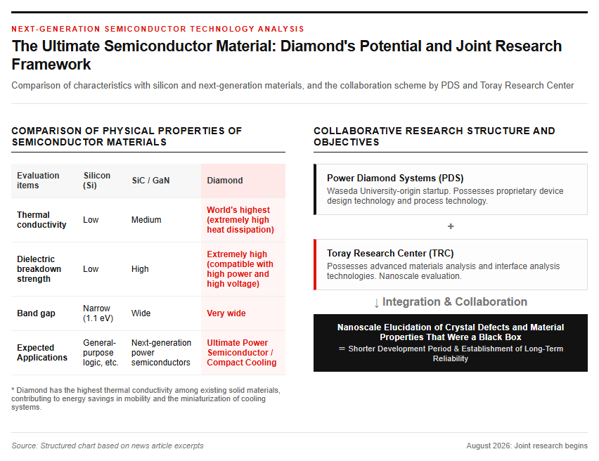
On August 20, 2026, Power Diamond Systems, Inc. (hereinafter “PDS”), a startup originating from Waseda University, and Toray Research Center, Inc. (hereinafter “TRC”) announced the commencement of a joint research project aimed at the practical application of diamond semiconductor devices, which are anticipated as next-generation semiconductors. Established in August 2022, PDS is a deep-tech startup dedicated to the research and development of power devices and other applications, built upon proprietary technology cultivated over many years by Professor Hiroshi Kawarada of Waseda University’s Faculty of Science and Engineering. This joint research will integrate TRC’s advanced material and interface analysis technologies with PDS’s proprietary device design and process technologies. Through this collaboration, the partners aim to systematically elucidate on a nanoscale how material properties and crystal defects—which have previously been a black box—affect device operation, thereby simultaneously achieving a dramatic reduction in development time and the establishment of long-term reliability as a product.
The Potential of Diamond as the Ultimate Semiconductor Material
Silicon carbide and gallium nitride are increasingly being adopted as next-generation materials to replace silicon, which is currently the mainstream in the semiconductor industry. However, diamond is considered the most promising candidate to shoulder the even more distant future. Diamond boasts the highest thermal conductivity of any existing solid material and is characterized by exceptionally superior heat dissipation compared to conventional silicon. In addition, its dielectric breakdown strength and bandgap—which corresponds to the energy gap—are extremely wide, demonstrating high durability even against large currents and high voltages. Because of this, it is most anticipated for application as a power semiconductor that efficiently converts and controls electrical power. Since cooling systems such as cooling fans can be miniaturized and made lightweight to the utmost limit, a significant improvement in energy-saving efficiency in the mobility field becomes possible. It holds numerous outstanding physical characteristics truly worthy of being called the ultimate semiconductor. Please refer to the figure below.
Technical Challenges Toward Practical Application and Joint Research Approaches
The Wall of Nanoscale Crystal Defects Impeding Practical Application
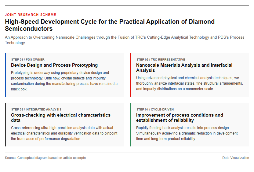
While diamond semiconductors theoretically demonstrate overwhelmingly high performance, numerous complex technical challenges stand in the way of their actual commercialization. The biggest bottleneck is the control of ultrafine crystal defects and impurities present inside the material or at its interfaces. In the manufacturing process of synthetic diamond and the device processing steps, microscopic structural disorders at an invisible level, the incorporation of unwanted impurities, and defects caused by thermal stress inevitably occur. These defects not only significantly impair the electrical characteristics of semiconductor devices, but also cause a decline in long-term reliability, such as operational variations and sudden failures during long-term use. Until now, an advanced mechanism to quantitatively evaluate what kind of defects and to what extent they lead to device performance degradation and feed that back into process design has not been established, forcing development to be conducted largely by trial and error.
TRC’s Cutting-Edge Analytical Technology and Rapid Development Cycle
The defining feature of this collaborative research is the direct integration of TRC’s renowned nanoscale material analysis technology into PDS’s prototyping and manufacturing processes. Specifically, by fully leveraging TRC’s advanced physical and chemical analysis technologies, the interface states, microstructural arrangements, and impurity distributions of diamond semiconductors are thoroughly analyzed on a nanometer scale. By cross-referencing this ultra-high-precision analytical data with the device electrical characteristics and durability verification data actually measured on the PDS side, it becomes possible to pinpoint the true substances or crystal structures causing performance degradation. This establishes a high-speed development cycle connecting material procurement, device prototyping, nano-level analysis, and the improvement of process conditions, which will dramatically accelerate overcoming performance variations and improving yields that previously required a considerable amount of time. Please refer to the figure below.
Future Developments and Expectations for Social Implementation
Ripple effects across diverse markets, including mobility and the space sector
When diamond semiconductors are successfully put into practical use, the field of transportation, which is undergoing rapid electrification, is expected to be the primary beneficiary. For example, in electric vehicles, incorporating diamond power semiconductors into quick-charging systems and high-efficiency motor drive inverters will achieve a dramatic reduction in overall system weight and power loss. Furthermore, diamond possesses the characteristic of having exceptionally high resistance to the intense radiation (cosmic rays) traversing outer space, compared to other semiconductor materials. Because of this, its application as a core device for communication systems and observation equipment on satellites operating in harsh space environments is also considered highly promising. It enables electronic control under high-voltage, high-current conditions or in extreme environments that had previously reached practical limits, holding a significant ripple effect that will fundamentally redefine the energy efficiency of industrial society as a whole.
Semiconductor Market Supremacy Led by Japan’s Proprietary Technology
PDS is built upon proprietary, Japan-origin licensed technologies, such as the hydrogen-terminated channel formation technology pioneered globally in 1994 by Professor Hiroshi Kawaharada of Waseda University, and the silicon oxide-terminated channel formation technology developed in 2020. While the semiconductor industry of the past was consumed by the race to manufacture the smallest chips, in today’s power semiconductor market, the source of competitiveness lies in how to manage the physical constraints of power and heat and optimize them for high efficiency. PDS is advancing its fabless operations by dynamically utilizing the state-of-the-art semiconductor manufacturing process equipment boasted by Waseda University. By further promoting strategic collaborations with major domestic and international semiconductor manufacturers and various research institutions, PDS will rapidly connect academic breakthroughs originating from Japan to societal implementation. Positioning this joint research as a solid stepping stone, PDS will command its unique value network and cement its technological superiority in the next-generation global semiconductor market.
Reference page
- [Toray Research Center News Release] https://www.toray-research.co.jp/news/article.html?contentId=fe6znhzh
- 【Power Diamond Systems】https://powerdiamondsys.com/
- [Waseda University Ventures] https://www.waseda.vc/
【#DiamondSemiconductor #PowerSemiconductor #Startup #WasedaUniversity #TorayResearchCenter #AdvancedTechnology】

コメント