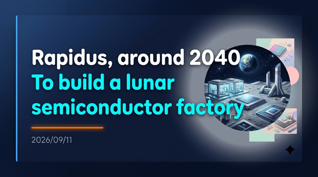
Rapidus, a company spearheading Japan’s efforts to domesticate next-generation semiconductor production, has unveiled a bold vision to construct a semiconductor fabrication plant on the Moon by around 2040. This plan is driven by the expansion of a lunar economy centered around the Artemis program, as well as the technical advantages of leveraging space’s unique physical environment for chip manufacturing.
- The 2040 Lunar Vision Unveiled in the U.S. and President Koike’s Strategic Intent
- Technical Advantages Offered by the Space Environment for Semiconductor Manufacturing
- Successful 2nm Trial Production in Chitose, Hokkaido and the Mass Production Roadmap
- Public-Private Support System and Fierce Competition in the Global Market
- Lunar Development Led by the Artemis Program and Expanding Semiconductor Demand
- Infrastructure, Transport Costs, and Harsh Environmental Challenges Toward 2040
The 2040 Lunar Vision Unveiled in the U.S. and President Koike’s Strategic Intent
Atsuyoshi Koike, President and CEO of Rapidus—the entity driving Japan’s domestic production of next-generation semiconductors—revealed the vision to build a semiconductor fabrication facility on the lunar surface by around 2040 during a speech at an event hosted by the Hudson Institute in New York on September 10, 2026. In his address, President Koike highlighted the presence of water resources on the Moon, essential for semiconductor manufacturing processes, emphasizing that “this is not a joke, but an extremely serious business plan.” An AI-generated concept video illustrating the lunar fab was screened at the venue, capturing significant attention from industry insiders and experts.
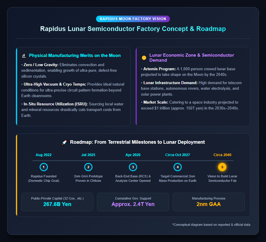
The following conceptual diagram illustrates the vision for the lunar semiconductor factory.
This ambitious project is backed by the rapid progress of crewed exploration and material transport initiatives to the Moon and Mars led by private space companies like SpaceX, headed by American entrepreneur Elon Musk. President Koike noted the movements of these private space ventures, explaining that his plan anticipates future reductions in space transport costs and advancements in lunar infrastructure. While manufacturing cutting-edge semiconductors presents formidable technical hurdles, presenting such an extreme target is also intended to inspire young engineers at Rapidus and ignite their passion for technological innovation.
Technical Advantages Offered by the Space Environment for Semiconductor Manufacturing
The concept of building a semiconductor factory on the Moon rather than on Earth offers unique physical and environmental benefits inherent to space and the lunar surface. First, in zero-gravity or microgravity environments, gravity-induced phenomena such as thermal convection and sedimentation—unavoidable on Earth—do not occur. This enables the ultra-uniform growth of high-purity silicon crystals used for semiconductor substrates, providing a clear technical advantage in refining high-quality materials with minimal crystal defects.
Furthermore, the ultra-high vacuum and cryogenic temperatures of space offer ideal conditions for processes forming hyper-precise circuit patterns. On Earth, cleanrooms consume vast amounts of energy and rely on complex equipment to remove airborne particles and artificially create vacuums. Directly utilizing space’s natural environment could dramatically boost production efficiency and quality. In addition, water and mineral resources essential for semiconductor raw materials exist on the Moon. If In-Situ Resource Utilization (ISRU) technologies develop to extract and process these materials locally, a sustainable manufacturing ecosystem could be established, drastically reducing material transport costs from Earth.
Rapidus’s Current Development Progress and Earthbound Challenges
Successful 2nm Trial Production in Chitose, Hokkaido and the Mass Production Roadmap
While holding a long-term perspective centered on a lunar fab, Rapidus’s immediate top priority remains establishing mass production technology on Earth for 2-nanometer generation cutting-edge logic chips. Established in August 2022, the company entered a strategic partnership with IBM for technology transfer, dispatching engineers to IBM’s research facility in Albany, New York, for joint development. As a result, in July 2025, Rapidus successfully prototyped and verified the operation of 2-nanometer semiconductor transistors employing the new Gate-All-Around (GAA) architecture at its manufacturing base in Chitose, Hokkaido.
The company began launching its pilot line in April 2025 and is making steady progress toward full-scale commercial production slated for around October 2027. In April 2026, Rapidus accelerated its manufacturing preparation by opening its back-end process facility, Rapidus Chiplet Solutions (RCS), and an analytics center within Seiko Epson’s Chitose plant. Furthermore, concrete order achievements with major Japanese corporations are accumulating: Fujitsu awarded Rapidus a manufacturing contract for 1.4-nanometer-class semiconductors aimed at supercomputers and domestic AI, while Canon entrusted the company with prototype production of image-processing semiconductors.
Public-Private Support System and Fierce Competition in the Global Market
Domesticating cutting-edge semiconductors is classified as a top-priority task for Japan’s economic security, backed by massive financial support from both the public and private sectors. In February 2026, capital investment from the Ministry of Economy, Trade and Industry (METI) and 32 private companies was finalized, bringing total public-private funding to 267.6 billion yen. From an initial base of 8 shareholders investing 7.3 billion yen at foundation, participation has broadened across automotive, electronics, and financial industries. Additionally, cumulative government support through initiatives like the Post-5G Fund Project has expanded to approximately 2.4 trillion yen.
However, the gap between Rapidus and its competitors in the global advanced semiconductor market remains dauntingly wide. World-leading foundry Taiwan Semiconductor Manufacturing Company (TSMC) and South Korea’s Samsung Electronics have already entered mass production for 2-nanometer processes, maintaining overwhelming advantages in yield improvement, equipment depreciation, and long-term contracts with major clients. Given the historical context of Japan’s semiconductor industry falling behind in the miniaturization race during the 40-nanometer generation, industry experts maintain a cautious outlook on whether Rapidus—lacking a proven track record and manufacturing know-how—can achieve sufficient yield rates and secure profitability.
Creation of a Lunar Economic Zone and Technical Hurdles to Overcome
Lunar Development Led by the Artemis Program and Expanding Semiconductor Demand
Rapidus’s lunar fab vision is closely aligned with global space development trends, including the U.S.-led Artemis lunar exploration program and industry blueprints like the Lunar Industry Vision (Planet 6.0). Under the Artemis program, in which the Japanese government participates, a crewed base accommodating 1,000 residents is projected to form on the lunar surface by the 2040s for water resource development and scientific exploration. As infrastructure such as communications base stations, autonomous rovers, water electrolysis systems, and solar power plants become operational on the Moon, demand for specialized chips to handle local high-level data processing and control will rise rapidly.
The global space industry market is projected to exceed \$1 trillion (approx. 150 trillion yen) between the 2030s and 2040s. Local data processing capabilities are indispensable for achieving local production and consumption of energy and information on the Moon. The lunar fab envisioned by Rapidus represents a strategic long-term initiative aiming to serve as core infrastructure in this future lunar economic zone.
Infrastructure, Transport Costs, and Harsh Environmental Challenges Toward 2040
Numerous technical and economic hurdles block the path to realizing a lunar fab by 2040. First, transporting heavy manufacturing equipment and ultra-precise instruments from Earth to the Moon remains astronomically expensive, making frequent, low-cost space transportation an indispensable prerequisite. Furthermore, shielding technologies must be developed to protect delicate factory equipment from intense cosmic radiation and extreme temperature fluctuations spanning hundreds of degrees between lunar day and night.
In addition, establishing sophisticated foundational technologies entirely different from those on Earth—such as securing a stable, high-capacity power supply for continuous plant operation and building efficient heat dissipation systems in a vacuum—is imperative. While the Japanese government supports private-sector technical demonstrations through its Space Technology Strategy and a 1-trillion-yen Space Strategy Fund, Rapidus must first succeed in mass-producing 2-nanometer semiconductors on Earth to prove its technological capability and economic viability as an absolute prerequisite.
Reference Pages
-
[Rapidus Corporation Official Website] https://www.rapidus.inc/
-
[JAXA Human Spaceflight Technology Directorate] https://humans-in-space.jaxa.jp/
-
[Cabinet Office Space Policy] https://www8.cao.go.jp/space/
-
[NASA In-situ Resource Utilization Overview] https://www.nasa.gov/overview-in-situ-resource-utilization/
[#Rapidus #Semiconductors #LunarDevelopment #SpaceBusiness #ArtemisProgram #NextGenTech #2nm]


コメント