A research team at the Korea Advanced Institute of Science and Technology (KAIST) has developed a next-generation phase-change memory device that reduces power consumption by approximately 15 times compared to conventional technology. This breakthrough comes against the backdrop of critical technological challenges: skyrocketing data center power consumption and heat dissipation demands driven by the global surge in AI adoption.
- The Arrival of Ultra-Low-Power Phase-Change Memory
- Mechanism of Self-Confined Nano-Filament Technology
- Features of Phase-Change Memory Combining the Best of DRAM and NAND
- Skyrocketing AI Data Center Power Consumption and Thermal Management Issues
- Applications in 3D Stacking and Neuromorphic Computing
- Structural Shifts in the Memory Industry and Key Outlook
The Arrival of Ultra-Low-Power Phase-Change Memory
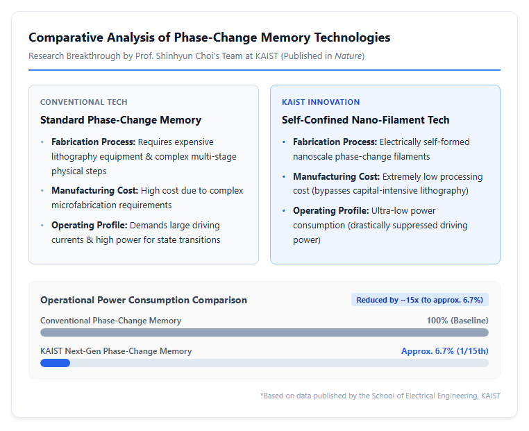
A research team led by Professor Shinhyun Choi from the School of Electrical Engineering at the Korea Advanced Institute of Science and Technology (KAIST) has successfully developed a next-generation phase-change memory device that dramatically lowers operational power consumption. Published on April 4, 2024, in the prestigious international journal Nature, these findings have drawn intense interest from both the semiconductor industry and academic communities worldwide. As generative AI and large language models (LLMs) proliferate rapidly, massive AI data centers are being built across the globe. However, the accompanying surge in energy consumption and severe thermal generation pose major obstacles to building sustainable AI infrastructure. In this global context, achieving such a drastic power reduction at the individual memory device level is hailed as a pivotal breakthrough capable of addressing energy bottlenecks in next-generation AI infrastructure. The new technology presented by the research team overcomes the physical limits of existing memory architectures, paving the way to balance high-performance computing with extreme energy conservation. Please refer to the figure below.
Mechanism of Self-Confined Nano-Filament Technology
The core technical innovation of this research lies in establishing an innovative method to electrically form self-confined, ultra-small nano-filaments. Traditionally, fabricating phase-change memory required expensive lithography equipment and complex, multi-stage physical processes to form ultra-fine structures, which led to high manufacturing costs and fundamental limits in improving power efficiency, thereby hindering widespread commercial adoption. However, Choi’s team devised a method that electrically self-forms nanometer-scale phase-change regions. This approach eliminates the need for capital-intensive equipment and complicated process steps, achieving an exceptionally low-cost fabrication process. Through this breakthrough technical approach, the team successfully suppressed operational power consumption down to an extreme fraction—roughly 1/15th of that required by existing phase-change memory produced with high-precision lithography. By simultaneously drastically reducing processing expenses and achieving ultra-low power consumption, this technique contributes significantly to harmonizing productivity with performance in memory manufacturing.
The “Power and Thermal Wall” in the AI Era and Its Technical Background
Features of Phase-Change Memory Combining the Best of DRAM and NAND
Phase-change memory is a next-generation memory technology that combines the ultra-fast read/write speeds of DRAM—the dominant memory medium today—with the non-volatile nature of NAND flash memory, which retains data even when power is turned off. It has been highlighted as a particularly promising candidate in neuromorphic computing, which mimics the complex neural networks of the human brain for efficient computation, as well as in next-generation storage architectures designed to eliminate data movement bottlenecks. Nevertheless, conventional phase-change memory required substantial driving currents during the phase transition between crystalline and amorphous states. Consequently, operational heat generation and power consumption remained excessively high, posing severe technical hurdles to capacity expansion, high-density 3D stacking, and large-scale deployment in practical commercial systems. The technological innovation achieved by KAIST serves as a crucial springboard for dramatically overcoming these long-standing high-power consumption issues inherent to phase-change memory.
Skyrocketing AI Data Center Power Consumption and Thermal Management Issues
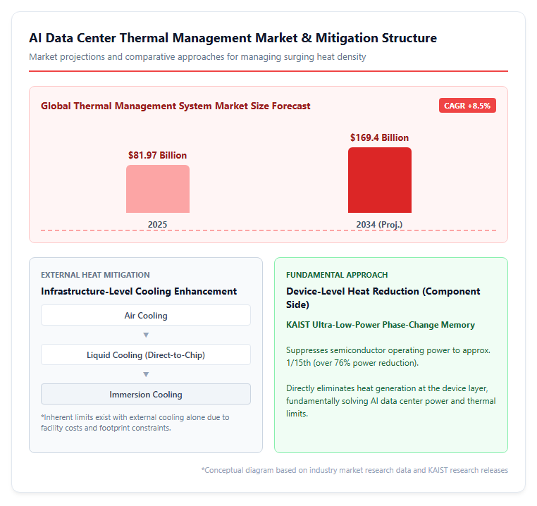
With the rapid acceleration of AI technology, controlling data center power consumption and the associated heat dissipation has evolved into both a global environmental issue and a national-scale industrial infrastructure challenge. According to market research data, the global thermal management system market is projected to grow from \$81.97 billion in 2025 at a compound annual growth rate (CAGR) of 8.5%, expanding to \$169.4 billion by 2034. Driven by the proliferation of high-density AI server clusters and High Bandwidth Memory (HBM), thermal density per rack has surged dramatically, accelerating investments in cooling infrastructure as facilities transition from air cooling to liquid cooling and immersion cooling methods. However, external thermal management solutions, such as cooling facilities, face inherent limits regarding cost and physical space. Thus, there is an urgent demand to fundamentally reduce heat generation and power consumption at the device level directly within semiconductor components. The low-power memory developed in this study offers a foundational solution to this pressing thermal management challenge. Please refer to the figure below.
Future Prospects for Practical Application and Expansion into Next-Generation AI Infrastructure
Applications in 3D Stacking and Neuromorphic Computing
The ultra-low-power phase-change memory developed by the KAIST team possesses a major structural advantage: a wide choice of compatible materials, making it remarkably easy to apply to high-density 3D stacked memory devices. Vertically stacking memory cells in vast numbers enables an explosive expansion of storage capacity per unit chip area. Furthermore, when incorporated as a building block for neuromorphic chips that replicate the synaptic connections of the human brain, it drastically cuts power losses caused by frequent data transfers between the CPU and memory in traditional Von Neumann computing architectures. This enables the construction of highly energy-efficient intelligent systems spanning from power-constrained edge AI devices—such as smartphones and drones—to mega-scale cloud data centers that process vast streams of data continuously.
Structural Shifts in the Memory Industry and Key Outlook
According to estimates by the World Semiconductor Trade Statistics (WSTS) and other industry analysts, the global semiconductor market reached approximately \$795.6 billion in 2025. In 2026, driven by aggressive data center investments by major tech corporations, the market is expected to expand rapidly to approximately \$1.5112 trillion. In this market environment, alongside leading advanced semiconductor technologies such as High Bandwidth Memory (HBM), CXL, and PIM, the commercial implementation of new-generation memory featuring ultra-low power consumption and low costs is eagerly anticipated. Looking ahead, the central focus will be on transitioning from laboratory-level technical validation to securing manufacturing yields in commercial production fabs and establishing smooth integration processes with major AI chipmakers and leading foundries. Toward realizing a sustainable AI-driven society, the industrial value and positive market impact brought by this innovative phase-change memory technology are immense.
Reference Pages
- 【KAIST Press Release】https://news.kaist.ac.kr/newsen/html/news/?mode=V&mng_no=36090
【#AIMemory #SemiconductorTechnology #KAIST #PhaseChangeMemory #EnergyEfficiency #NextGenTech #Neuromorphic #ElectricalEngineering】


コメント