Cognex has announced the new “In-Sight 1750 Series” wafer reader designed to enhance traceability in semiconductor manufacturing. The release is driven by chipmakers rapidly expanding their production capacity amid the soaring demand for AI infrastructure, alongside an increasing need for high-precision identification to prevent operational downtime during the manufacturing process.
- Key Points of the Event and Background of Development
- Key Technologies and Advanced Features of the In-Sight 1750 Series
- Reducing Downtime and Maximizing Throughput
- Easy upgrade and seamless integration from existing equipment
- The Growth of the Semiconductor Inspection and Metrology Equipment Market and the Importance of Defect Control
- Future Outlook and Key Points to Watch
Key Points of the Event and Background of Development
Cognex, a global leader in the industrial machine vision field, announced on September 23, 2026, the launch of the “In-Sight 1750 Series,” a next-generation wafer and panel identification system that significantly reduces operational downtime on semiconductor manufacturing lines while enhancing traceability and maintaining high throughput.
Currently, demand for global AI infrastructure construction, advanced data processing, and next-generation electronics is increasing at an accelerating rate, and major chipmakers are expanding their production capacity at an unprecedented speed. In manufacturing processes ranging from semiconductor front-end to back-end operations and advanced packaging, reliably reading each wafer’s identification numbers and marks and correctly managing its manufacturing history are key to maintaining yields.
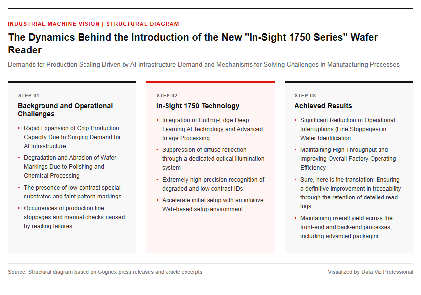
However, in actual manufacturing environments, there are numerous wafers with degraded markings due to polishing or chemical processing, as well as special substrate materials with low contrast. Even a single reading failure can cause the production line to temporarily halt or necessitate manual verification work, severely impacting the overall operational efficiency of the factory. The newly announced In-Sight 1750 is the latest wafer identification system developed to solve these pressing challenges on the manufacturing floor.
Key Technologies and Advanced Features of the In-Sight 1750 Series
The In-Sight 1750 series is a system that highly integrates Cognex’s long-cultivated expertise in the field of wafer identification with the latest deep learning AI technology, advanced image processing algorithms, and a custom-designed optical illumination system.
It has become possible to read IDs with extremely high precision through AI-powered image analysis, even for heavily degraded or scratched marks, surface structures prone to diffuse reflection, and faint pattern engravings that were difficult to recognize with conventional optical identification devices.
In addition, the user interface adopts a new Web-based setup environment, which eliminates the need for complex optical adjustments or programming, allowing initial settings and parameter changes to be completed in a short time. Furthermore, a major feature is that the device is equipped with a detailed reading log retention function inside, enabling the accurate tracking and accumulation of traceability data during the manufacturing process.
For the installation image of the device and its actual operational status, please refer to the following images.
This system functions as a powerful infrastructure to promote the automation of quality management and ensure consistency in process control.
Benefits of Implementation and Innovativeness in Semiconductor Manufacturing Environments
Reducing Downtime and Maximizing Throughput
By introducing this system in semiconductor manufacturing plants, chipmakers can minimize manual troubleshooting and intervention by operators. By reducing the frequency of line stoppages caused by identification errors, the overall operating rate of wafer processing equipment is significantly improved, which directly contributes to maintaining overall factory throughput.
Matt Moschner, President and CEO of Cognex, pointed out that massive investments in AI infrastructure are driving unprecedented expansion across the entire semiconductor industry, emphasizing the importance of rapidly launching new lines without sacrificing quality and traceability in any way. The In-Sight 1750 is designed precisely as the optimal solution to meet such demanding requirements.
Furthermore, maintaining reliable individual identification across all stages—from front-end wafer processing to back-end dicing, advanced packaging, and final testing—accelerates root cause analysis when defects occur, offering the significant benefit of substantially shortening the feedback cycle for process improvement.
Easy upgrade and seamless integration from existing equipment
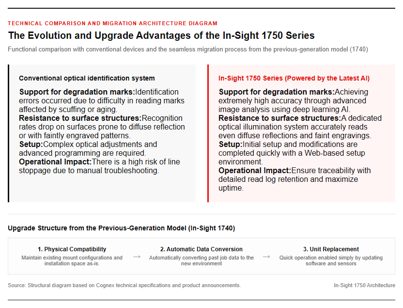
In production line renovations, it is necessary to avoid downtime and the risk of large-scale design changes associated with upgrading existing equipment as much as possible. The In-Sight 1750 series is designed to allow existing users currently operating the previous-generation “In-Sight 1740” to transition smoothly.
Specifically, it features an automatic conversion function for previously created job data, allowing the upgrade to a next-generation AI identification environment to be completed simply by replacing the software and sensor unit, without changing the physical installation space or mounting configuration. This enables manufacturers to obtain the latest image recognition performance while minimizing the impact on their daily operations.
The overall system structure and wiring configuration are as shown in the following diagram.
Thus, the flexibility to keep the barrier to entry as low as possible while dramatically enhancing on-site productivity and traceability is one of the reasons why it is so highly regarded by semiconductor manufacturers.
Industry Trends and Future Technical Outlook
The Growth of the Semiconductor Inspection and Metrology Equipment Market and the Importance of Defect Control
As the miniaturization and high integration of product structures progress in the semiconductor industry, the importance of defect inspection, identification, and measurement technologies is growing year by year. According to market research data, the global semiconductor inspection and metrology equipment market is projected to grow from $17.2 billion in 2025 to $19.7 billion in 2026, and reach $29.8 billion by 2032. The compound annual growth rate (CAGR) over this period is estimated at approximately 7.14%, supporting the steady overall growth of the industry.
With not only the miniaturization of circuit line widths, but also the adoption of GAA (Gate-All-Around) structures, the multi-layering of 3D NAND, and advancements in advanced packaging technology integrating HBM (High Bandwidth Memory), microscopic defects and pattern misalignment occurring on wafers have come to inflict extremely serious damage on yields. Consequently, identification equipment that instantly pinpoints and tracks the location of defects and the target wafers is no longer a mere complementary tool, but has transformed into core infrastructure supporting wafer fab operations and yield optimization.
Future Outlook and Key Points to Watch
Moving forward, the adoption of a hybrid architecture combining instant identification processing on edge devices with advanced AI model training and centralized data management in cloud environments is expected to accelerate even further. Rather than relying on standalone identification devices, solutions that seamlessly integrate in real time with factory-wide MES (Manufacturing Execution Systems) and yield management databases will likely become mainstream in the market.
Furthermore, along with moves to strengthen regional supply chains and build new factories in major manufacturing regions such as mainland China, South Korea, Taiwan, and North America, procurement demand for state-of-the-art identification systems compatible with automation and smart technologies is expected to expand even further going forward.
Whether [they] can integrate highly sensitive identification technology, high throughput, and an easy-to-use software environment will be the key to determining the competitiveness of equipment manufacturers. Future market trends will be closely watched to see how the introduction of the new-generation wafer reader will contribute to the global mass production and yield improvement of AI semiconductors.
Reference page
- [Cognex – In-Sight 1750 Series Product Information] https://www.cognex.com/ja/products/2d-machine-vision-systems/in-sight-1750
【#Cognex #InSight1750 #SemiconductorInspection #WaferReader #MachineVision #AITec #Traceability #YieldImprovement】

コメント