Israel-based Tower Semiconductor has unveiled a major investment plan exceeding 600 billion yen in Japan. The move is driven by surging demand for faster data transmission in generative AI applications and economic security imperatives to mitigate geopolitical risk.
- Major METI Subsidies and the Scope of the Investment
- A Two-Stage Production Expansion Roadmap across Niigata and Toyama
- Overcoming the “Copper Bottleneck” in AI Data Centers
- Technical Advantage in Silicon Photonics and Specialty Foundry Process
- Mitigating Geopolitical Risk and Restructuring Global Supply Chains
- Regional Economic Impact and Key Milestones to Watch
Major METI Subsidies and the Scope of the Investment
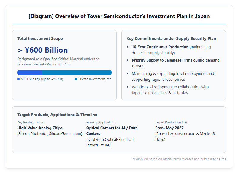
On July 14, 2026, Tower Semiconductor, a leading Israeli specialty foundry, announced a large-scale expansion plan in Japan. The total project footprint exceeds ¥600 billion, supported by up to approximately ¥159 billion in subsidies from the Japanese government under its Economic Security Promotion Act. Designating semiconductors as a “specified critical material,” Japan aims to bolster its domestic supply chain for key advanced technologies. Notably, this investment does not target leading-edge compute chips, but rather high-value-add analog semiconductors, such as silicon photonics (SiPho) and silicon germanium (SiGe) used in optical communications. Under a supply security agreement with the Ministry of Economy, Trade and Industry (METI), Tower has committed to maintaining production in Japan for at least ten years and prioritizing supplies to Japanese companies during demand surges. This government backing seeks to establish a resilient supply base while upgrading Japan’s broader digital infrastructure. Please refer to the following diagram:
A Two-Stage Production Expansion Roadmap across Niigata and Toyama
The investment plan follows a dual-track strategy to systematically scale manufacturing capacity. Under Stage 1, Tower will convert its Arai Plant (formerly Fab 6) in Myoko, Niigata Prefecture, into a dedicated hub for 300mm silicon photonics and advanced packaging, with initial shipments targeted for May 2027. Concurrently, it will expand 300mm capacity at Fab 7 in Uozu, Toyama Prefecture, building out volume production readiness by the fourth quarter of 2027. Under Stage 2, Tower plans to construct a new 300mm manufacturing facility adjacent to Fab 7, aiming to complete the buildout in 2028 and drive significant revenue contribution starting in 2029. Furthermore, Tower is restructuring its TPSCo joint venture with Taiwan’s Nuvoton Technology, acquiring full ownership of the Uozu plant to specialize strictly in 300mm wafer fabrication. Combined across both sites, monthly output is projected to reach 18,000 12-inch wafer equivalents, creating one of the world’s largest manufacturing hubs for silicon photonics.
Optical Semiconductor Technology and Silicon Photonics Powering the AI Era
Overcoming the “Copper Bottleneck” in AI Data Centers
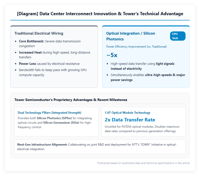
With the explosive growth of generative AI, hyper-scale data centers worldwide face critical challenges around power consumption and bandwidth constraints. In traditional electronic architectures, moving massive volumes of data across GPUs and servers over copper wiring creates severe data latency, excessive heat generation, and substantial power loss. Silicon photonics—the core of optical-electrical integration—has emerged as a game-changing technology to break through this physical barrier. By integrating optical circuits onto silicon substrates, information is transmitted using light rather than electrical signals, enabling ultra-high-speed communication alongside dramatic power reductions. Major chipmakers like NVIDIA are aggressively shifting toward optical interconnects, projecting a roughly 5-fold improvement in power efficiency through Co-Packaged Optics (CPO) compared to conventional pluggable transceivers. As compute capabilities expand, optical semiconductors that transport data have become just as vital as the logic chips doing the processing.
Technical Advantage in Silicon Photonics and Specialty Foundry Process
Tower Semiconductor holds a leading global market share in analog semiconductors for optical communications. Beyond silicon photonics, the company possesses proprietary silicon germanium (SiGe) technology for high-frequency analog circuits, giving it a unique advantage in seamlessly integrating optical signals with electronic controls. In February 2026, Tower announced next-generation SiPho technology supporting 1.6T (Terabit) optical modules for NVIDIA, doubling data transfer rates compared to previous generations. In Japan, Tower is also collaborating on joint R&D and deployment for NTT’s next-generation IOWN (Innovative Optical and Wireless Network) initiative. Even without relying on sub-nanometer logic nodes, Tower’s mastery over specialized process technologies makes it an indispensable player shaping the performance and scalability of AI infrastructure. Please refer to the following diagram:
Geopolitical Risk Diversification and Outlook
Mitigating Geopolitical Risk and Restructuring Global Supply Chains
For Tower, expanding its footprint in Japan serves as a pivotal strategic move to hedge against rising geopolitical risks stemming from Middle East tensions. Establishing heavy volume production in Japan—a region offering reliable power supplies and mature industrial infrastructure—provides global customers with essential supply continuity. The strategic agility of Tower’s Japanese footprint was recently underscored when production allocated under a former arrangement with Intel was rapidly redirected to Toyama’s Fab 7 following arbitration over contract fulfillment. With its Japanese expansion as a cornerstone, Tower has set an ambitious 2028 financial target of \$3.6 billion in revenue and \$1.2 billion in net profit. By scaling its foundry operations in Japan, the company is positioning itself to lead the realignment of the global semiconductor supply chain.
Regional Economic Impact and Key Milestones to Watch
The ¥600 billion investment is expected to generate significant economic ripple effects and high-tech employment across the Hokuriku region (Niigata and Toyama). Tower is actively partnering with Toyama University, local technical colleges, and vocational schools to foster advanced engineering talent and collaborate on applied research. By embedding itself within local educational and industrial networks, Tower reduces exit risks often associated with foreign investments, building a durable ecosystem that retains skills and jobs locally over the long term. Looking ahead, key milestones will include meeting fab construction timelines, executing the ten-year continuous production commitment, and honoring priority supply agreements for domestic Japanese firms. The ultimate test will be whether public subsidies can serve as an effective catalyst to unlock autonomous private investment and sustained technological innovation. Building a global optical semiconductor hub in Hokuriku represents a major test case for revitalizing Japan’s chip industry and securing economic sovereignty.
Reference Pages
- 【Tower Semiconductor Press Release】https://jp.towersemi.com/2026/07/14/07142026/
- 【Ministry of Economy, Trade and Industry Approved Plan】https://www.meti.go.jp/policy/economy/economic_security/semicon/nintei_anpohandoutai_keikaku_29.pdf
【#Semiconductors #SiliconPhotonics #TowerSemiconductor #EconomicSecurity #OpticalIntegration #AIDataCenters #RegionalRevitalization】
コメント