NVIDIA has announced “NVHBM,” a groundbreaking technology designed to elevate the performance of AI accelerators. This move comes as memory bandwidth and power consumption in High Bandwidth Memory (HBM) have become severe bottlenecks in AI processing.
- The Driven Need for Base Die Redesign to Overcome AI Bottlenecks
- Expanding Compute Capacity and Die Area Through a 67% Footprint Reduction
- Transforming Data Centers with a 30% Bandwidth Boost and 15% Power Savings
- Strategic Impact on Inference Workloads and Massive AI Scale
- Shifting Control in Custom HBM and Major Vendor Strategies
- Soaring Memory Costs, Tight Supply, and the AI Roadmap to 2030
The Driven Need for Base Die Redesign to Overcome AI Bottlenecks
As AI models continue to expand exponentially, memory bandwidth has emerged as the primary bottleneck limiting overall processing performance. To fundamentally address this challenge, NVIDIA unveiled “NVHBM” in August 2026—a innovative technology developed and validated in close collaboration with major memory suppliers. NVHBM introduces a newly customized building block that completely redesigns the base die located at the bottom of the High Bandwidth Memory (HBM) stack. In traditional HBM architecture, the memory controller resides on the host processor side, such as the GPU or XPU. The key architectural shift in NVHBM lies in relocating and integrating this memory controller directly into the HBM stack’s base die. While base dies previously played a limited role in managing signals between DRAM dies and GPUs, NVHBM elevates the base die into an advanced command center functioning as a logic chip. This pioneering approach is scheduled for its first global implementation in Trainium 4, the next-generation AI training chip developed by Amazon’s Annapurna Labs. It is expected to deliver unprecedented improvements in processing speed and operational efficiency, particularly for memory-bound workloads such as AI inference and massive Large Language Model (LLM) operations.
Expanding Compute Capacity and Die Area Through a 67% Footprint Reduction
The circuit design innovations underpinning NVHBM provide substantial physical footprint advantages at the chip package level. Alongside moving the memory controller to the base die, NVHBM adopts a custom PHY interface with a significantly narrower footprint than conventional designs. This architectural refinement slashes the physical area required by the PHY and its supporting circuitry by up to 67%. Furthermore, simplifying the wiring topology on the interposer connecting heterogeneous dies increases the usable silicon footprint on the same chip package by up to 80%. Please refer to the diagram below.
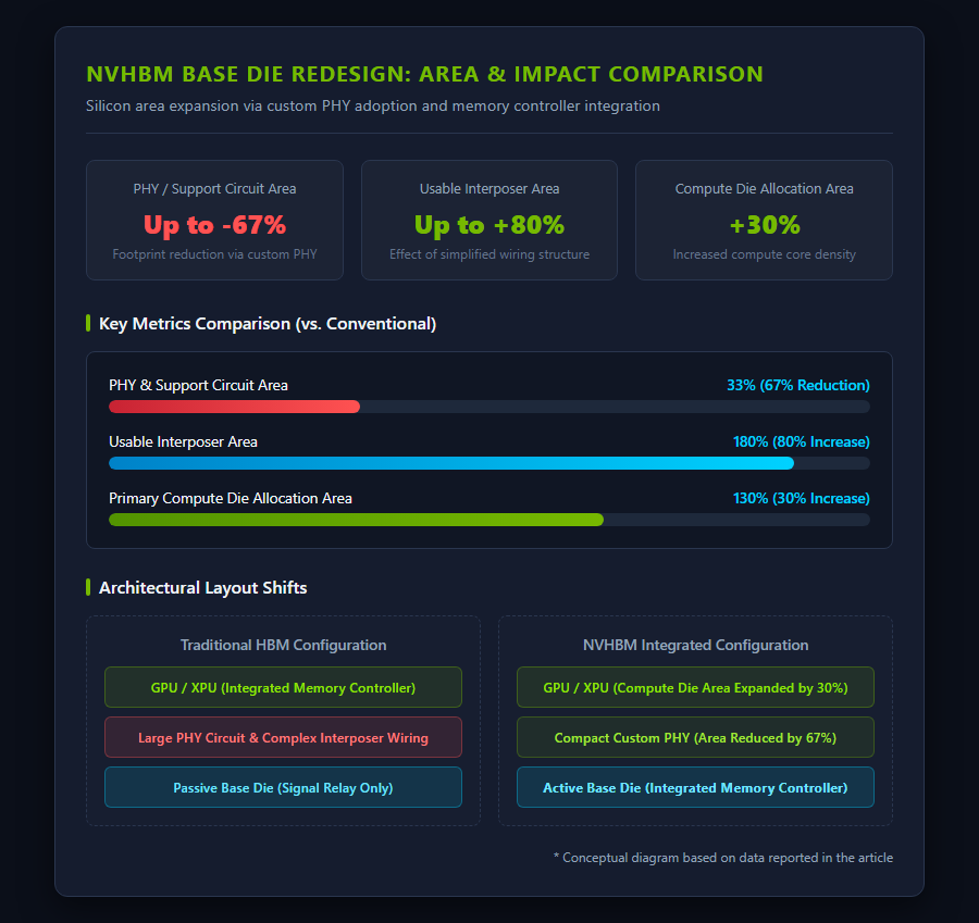
By capitalizing on this expanded substrate space, the allocation area for the primary compute die responsible for core processing tasks can expand by 30% compared to previous generations. This dramatic increase in logic circuit and compute unit density allows a single AI accelerator to accommodate a far broader set of functional units. By overcoming physical layer constraints through structural redesign, NVHBM’s architecture is widely recognized as a major milestone in next-generation semiconductor packaging.
Delivering Unmatched Performance: A 30% Bandwidth Boost and Lower Power
Transforming Data Centers with a 30% Bandwidth Boost and 15% Power Savings
The performance gains achieved by NVHBM are remarkable. Compared to next-generation HBM4E industry standards, NVHBM increases memory bandwidth by up to 30% per stack. Simultaneously, operational power consumption is reduced by 15% relative to HBM4E, successfully resolving the traditional trade-off between higher processing speeds and energy efficiency. When paired with NVIDIA’s proprietary high-speed interconnect technology, NVLink Fusion, communication between the XPU and other platform components reaches peak throughput, driving an end-to-end performance gain of up to 30% per XPU.
A 15% reduction in power consumption carries immense operational significance for hyperscale data centers. For instance, in a large-scale data center facility operating 2,000W-class XPUs, the power saved can free up enough energy capacity to power up to 15,000 additional compute nodes. Furthermore, this efficiency substantially reduces thermal and electrical loads on rack-level cooling and power distribution systems, directly contributing to a lower total cost of ownership (TCO) across data center infrastructure.
Strategic Impact on Inference Workloads and Massive AI Scale
This transition to next-generation memory relies on the significant technological leaps embodied in the HBM4 generation as a whole. The HBM4 architecture doubles the number of independent data transmission channels from 16 to 32, fundamentally strengthening parallel transfer capacity. Additionally, silicon die stacking reaches up to 16 DRAM layers, providing the ultra-high memory capacities required to store the massive parameter counts of frontier AI models. Please refer to the structural diagram below.
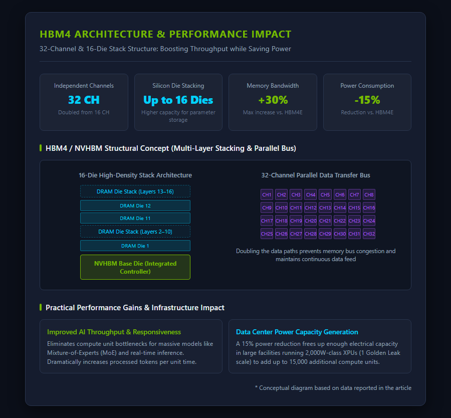
In practical deployment, this combination of higher bandwidth and expanded capacity dramatically improves overall AI throughput. Heavy workloads—such as Mixture-of-Experts (MoE) architectures that combine multiple specialized sub-models, or real-time AI inference services—have historically suffered severe performance degradation due to memory bus congestion. By ensuring a continuous, high-speed stream of data directly to the compute units, NVHBM prevents data starvation, dramatically boosting token processing rates and query response throughput across existing data center footprints.
The HBM4 Market Tug-of-War and Future AI Infrastructure Outlook
Shifting Control in Custom HBM and Major Vendor Strategies
The arrival of NVHBM is reshaping the competitive dynamics between memory vendors and chip designers across the semiconductor industry. Historically, memory specialists such as Samsung Electronics and SK Hynix maintained control over base die design and fabrication. Under the NVHBM architecture, however, processor design leaders like NVIDIA are stepping forward to lead memory controller integration and logic circuit customization.
This shift has intensified competition among major suppliers vying for leadership in the HBM4 era. SK Hynix, holding roughly 50% of the global HBM market share, has formed a strategic alliance with foundry giant TSMC to advance HBM4 base die manufacturing using leading-edge logic processes. Meanwhile, Samsung Electronics is leveraging its turn-key “one-stop” model—spanning logic, memory, foundry, and advanced packaging—and achieved top marks for speed and power efficiency during NVIDIA’s rigorous HBM4 qualification testing (SiP testing). Micron is also targeting mass production with bandwidth capabilities exceeding 2.8 TB/s, setting the stage for a fierce three-way contest.
Soaring Memory Costs, Tight Supply, and the AI Roadmap to 2030
The AI infrastructure market is expected to face prolonged supply tightness and rising component costs over the coming years. According to market research firm TrendForce, DRAM contract prices experienced historic surges, jumping 90% to 95% quarter-over-quarter in Q1 2026, followed by an additional 58% to 63% increase in Q2. NVIDIA Chief Financial Officer Colette Kress acknowledged that sharply rising memory prices have placed temporary pressure on gross margins, while revealing that the company doubled its purchase commitments to \$279 billion to lock in future memory supply.
SK Hynix leadership anticipates that the multi-year lead times required to construct massive wafer fabrication complexes will keep market supply tight until at least 2030. As a result, the delivery schedule for next-generation accelerators—including NVIDIA’s Vera Rubin AI platform scheduled for market launch in late 2026—depends directly on securing sufficient HBM supply. NVIDIA’s dual strategy of aggressive supply chain commitments and structural memory redesign will serve as a crucial factor determining the pace of global AI infrastructure deployment.
Reference Pages
- [State Administration for Market Regulation (SAMR) Official Announcement] https://www.samr.gov.cn/xw/zj/art/2025/art_66b8363c3a194ba0a394a843d6cf3fd1.html
【#NVIDIA #NVHBM #HBM4 #AISemiconductors #MemoryTechnology #DataCenter #PowerEfficiency】


コメント