In improving semiconductor manufacturing yields, a new approach that fuses large language models (LLMs) with conventional AI (machine learning and symbolic AI) is rapidly expanding. This trend is driven by the rise of advanced nodes and complex 3D packaging, making technologies that combine textual explanations and causal verification with numerical analysis indispensable.
- Key Points of the Event and Overview of LLM-Conventional AI Integration
- Wafer Defect Analysis Using Vision-Language Model WaferSAGE
- Neuro-Symbolic AI and the Pursuit of Verifiability
- Preventive Control via Virtual Simulation and Time-Series AI
- Limitations and Challenges of Analysis in Advanced Packaging
- Future Developments Toward On-Site Implementation and the Importance of Data Standardization
Key Points of the Event and Overview of LLM-Conventional AI Integration
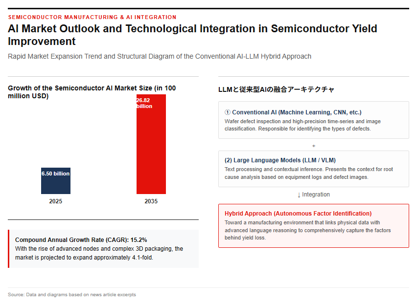
The AI market in semiconductor manufacturing is expanding rapidly, and is projected to grow from $6.50 billion in 2025 to $26.82 billion by 2035 (at a compound annual growth rate of 15.2%). In conventional wafer defect inspection and yield management, traditional AI technologies such as convolutional neural networks (CNNs) have been responsible for pattern classification. However, these methods only identify defect types, making it difficult to pinpoint the exact location of occurrence or provide contextual root-cause analysis. To address these challenges, hybrid approaches combining traditional AI with large language models (LLMs) and vision-language models (VLMs) are gaining attention. By fusing the high-precision time-series and image classification capabilities of traditional AI with the text processing and reasoning capabilities of LLMs, a framework is emerging to comprehensively capture the factors behind yield degradation from both equipment logs and defect images. At semiconductor fab sites, the shift is progressing from the introduction of standalone inspection tools to advanced manufacturing environments that autonomously identify factors and provide recommendations. The architectural diagram connecting on-site physical data with advanced linguistic reasoning is shown below.
Wafer Defect Analysis Using Vision-Language Model WaferSAGE
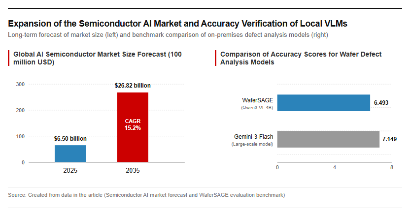
To break through the barriers of data scarcity and confidentiality in wafer defect image analysis, a new technology called “WaferSAGE” has been proposed. Because semiconductor fabs strictly restrict sending images to external cloud APIs, the use of small, locally running VLMs is essential. WaferSAGE uses ViT and K-Means clustering to remove label noise from public datasets such as WM811K and MixedWM38. It then automatically generates an evaluation rubric specifying “essential keywords” and “avoidance keywords” from three perspectives: spatial arrangement, morphology, and root cause. As a result of applying reinforcement learning (GSPO) based on this rubric, the Qwen3-VL model with only 4 billion parameters (4B) recorded a score of 6.493, achieving response accuracy approaching that of the larger Gemini-3-Flash model (7.149). It demonstrates exceptional feature separation capability, particularly in complex defects where center defects and scratches are mixed, showing that practical defect analysis is achievable in on-premises environments.
Neuro-Symbolic AI and the Pursuit of Verifiability
There is a growing movement pointing out that “LLMs alone are insufficient” for yield improvement and advocating instead for neuro-symbolic AI. Satya Nitta and colleagues at Emergence AI propose an approach that integrates LLMs, which generate text probabilistically, with rule-based symbolic AI. Semiconductor manufacturing is a mission-critical environment, where incorrect root cause analysis or recipe changes risk causing massive financial damage. To address this, they built a mechanism that deploys symbolic AI as a validation layer to deterministically verify whether the explanations and hypotheses presented by the LLM comply with physical laws and manufacturing rules. This integrated system aims to safely and reliably increase the number of good chips per wafer. Below is a conceptual diagram combining AI agents running in a local fab environment with symbolic verification.
Advanced AI Methods, Challenges, and Future Prospects in Fab Operations
Preventive Control via Virtual Simulation and Time-Series AI
A transition is underway from conventional experimental cycles that consume physical wafers to advanced control utilizing digital twins and predictive AI. Developed by Lam Research, the Fabtex Yield Optimizer analyzes SEMulator3D virtual silicon models and in-line metrology data using AI/ML to calculate optimal process target values. Compared to conventional sequential trial-and-error experiments using Pareto analysis, it has succeeded in proactively predicting complex defects spanning multiple processes on 3D structures, significantly reducing development time and wafer waste costs. In addition, in contrast to conventional Statistical Process Control (SPC), which issues alerts only after control limits are exceeded, “proactive SPC” using time-series forecasting AI such as N-BEATS has also emerged. By anticipating future measurement values and detecting deviations in advance, a system is being established to adjust equipment settings and perform preventative interventions before defective wafers are produced.
Limitations and Challenges of Analysis in Advanced Packaging
The expansion of advanced packaging, represented by chiplets, 3D packaging, and hybrid bonding, is bringing new physical limits to yield analysis. According to an industry survey conducted by the University of Florida, the importance of failure analysis (FA) for packaging and heterogeneous integration was rated 7.92 out of 10, making it a strategic challenge that surpasses traditional standalone device analysis. In particular, 54% of respondents cited hybrid bonding as the “most difficult new structure to analyze,” with the detection of interfacial voids and misalignments, as well as the management of substrate warpage caused by thermal stress, posing major barriers. To avoid the risk of defect traces being destroyed during sample preparation, 72% of the industry is demanding improvements in non-destructive testing methods, with a strong, eager desire for the integration of non-destructive observation technologies such as high-resolution 3D X-ray imaging (rated 8.18) and AI-powered image analysis.
Future Developments Toward On-Site Implementation and the Importance of Data Standardization
The biggest key to successfully establishing semiconductor yield improvement AI in actual production lines lies in multimodal data standardization and infrastructure development. According to a survey, 83% of experts advocate for the necessity of a data standardization framework in heterogeneous material integration, and building a data infrastructure that handles electrical tests, physical observation, and process history in an integrated manner is considered essential. Furthermore, since anomaly data generated within fabs is extremely rare—accounting for less than 0.1% of the total—”unsupervised anomaly detection” trained only on normal data and “RAG-based LLM agents” are becoming the de facto standard. LLMs function as conversational interfaces responsible for knowledge extraction and transfer, significantly shortening the ramp-up period for newcomers by converting the tacit knowledge of veteran engineers into explicit knowledge. Moving forward, the construction of digital twin infrastructure connecting everything from design to manufacturing and inspection in a closed loop is expected to progress, realizing a preventive and sustainable yield improvement system.
Reference page
- [WaferSAGE VQA Dataset] https://huggingface.co/datasets/Niraya666/wafermap-vqa-2602
- 【Fabtex Yield Optimizer – Lam Research】https://www.lamresearch.com/product/fabtex-yield-optimizer/
- 【Intelligent Assistants for Semiconductor FA with LLM-Based Planning Agents】http://arxiv.org/abs/2506.15567v3
- 【Unsupervised Anomaly Prediction with N-BEATS and GNN】http://arxiv.org/abs/2510.20718v1
- 【Proactive Statistical Process Control Using AI】http://arxiv.org/abs/2509.16431v1
【#Semiconductors #YieldImprovement #LLM #ArtificialIntelligence #WaferSAGE #DigitalTwin #FailureAnalysis】


コメント