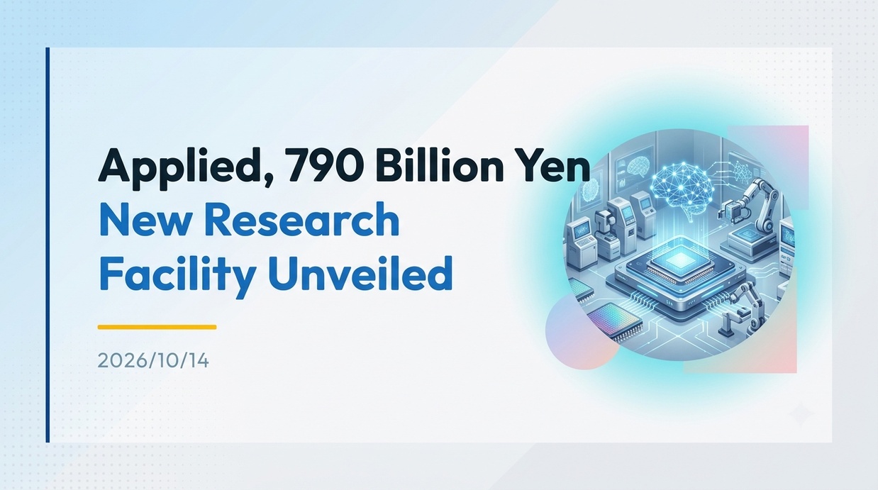
US-based Applied Materials has unveiled the “EPIC Center,” a collaborative semiconductor R&D facility with a total investment of approximately $5 billion, in Silicon Valley. Behind this initiative are challenges such as the increasing complexity of chip design accompanying the rapid expansion of the AI market, and delays in ramping up mass production using conventional development models.
- The Full Picture and Facility Scale of the EPIC Center, Which Revolutionizes the Traditional Model
- Formation of an ecosystem bringing together major semiconductor players
- Competition and Collaboration Surrounding Next-Generation Logic and 3D Stacking Technology
- Breaking Bottlenecks through Memory Densification and Advanced Packaging
- Acceleration of Cutting-Edge Process Development and Market Growth Forecast
- Supply Chain Constraints and Compliance Management Challenges
The Full Picture and Facility Scale of the EPIC Center, Which Revolutionizes the Traditional Model
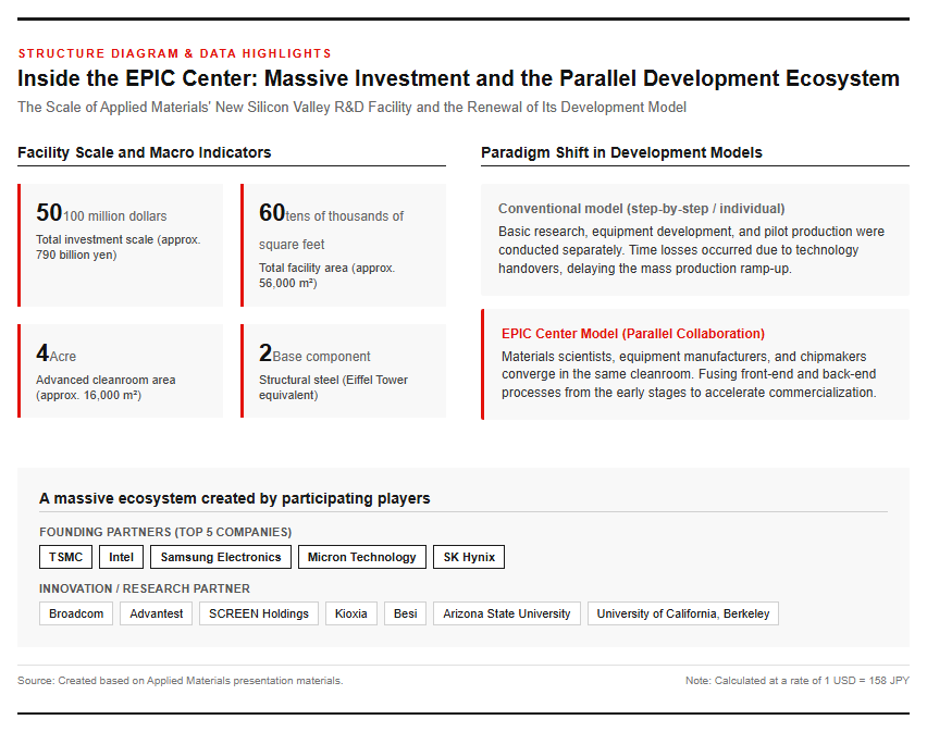
Applied Materials, the world’s largest semiconductor manufacturing equipment maker, unveiled the “EPIC Center” in Sunnyvale, California, USA on October 12, 2026. The investment amount is expected to expand in stages along with the rollout of customer projects, reaching a total scale of approximately $5 billion (approx. 790 billion yen, calculated at 1 dollar = 158 yen). The facility size spans 600,000 square feet (approx. 56,000 square meters), with the advanced cleanroom occupying about 4 acres (approx. 16,000 square meters). It took a total of over 6 million construction hours to complete, with the foundation using enough concrete to fill 34 Olympic-sized swimming pools and the structure using steel equivalent to two Eiffel Towers. Please refer to the diagram below for the internal layout of the facility.
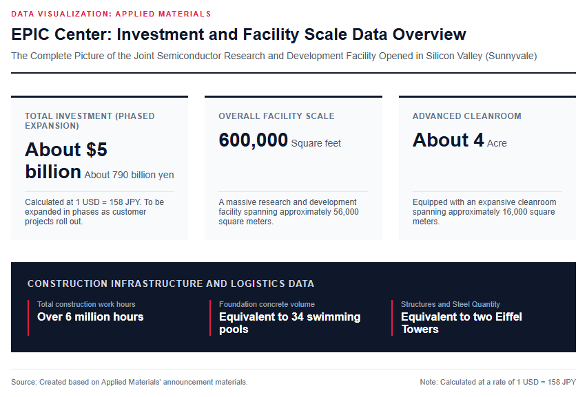
This facility was designed to eliminate the conventional phased development model, in which basic materials research, equipment development, and pilot production are conducted separately. By bringing materials engineering researchers, equipment manufacturers, and chipmakers together in the same cleanroom to conduct parallel development, it dramatically shortens the timeline from prototyping to mass production.
Formation of an ecosystem bringing together major semiconductor players
The EPIC Center features broad participation from companies and research institutions driving the global semiconductor ecosystem. Its founding partners include the five major companies TSMC, Intel, Samsung Electronics, Micron Technology, and SK Hynix. In addition, Broadcom, Advantest, SCREEN Holdings, Kioxia, and Besi participate as innovation partners, while prominent universities such as Arizona State University and the University of California, Berkeley participate as research partners. Please refer to the figure below for the correlation structure of the participating companies.
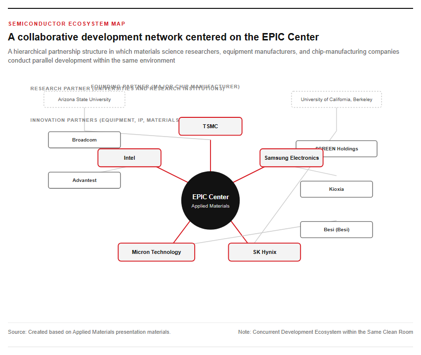
Each partner company stations its specialized engineers on-site in an environment where their intellectual property is protected, working directly with Applied Materials’ teams. By integrating front-end process development with back-end test and measurement technologies from the initial stages, technology optimization prior to mass production becomes possible. This prevents time loss associated with separate technology handoffs, establishing a framework that fundamentally accelerates the speed of technology commercialization in the AI era.
Co-Development and Innovation of Chip Technologies Demanded by the AI Era
Competition and Collaboration Surrounding Next-Generation Logic and 3D Stacking Technology
In the development of next-generation AI chips, realizing ultra-fine processes of 2 nanometers or less and three-dimensional stacked architectures has become the most critical challenge. It is groundbreaking that TSMC and Intel, which are competitors in the foundry market, are participating side by side at the same research hub. Building on a 30-year partnership, TSMC will advance the joint development of new materials, low-resistance wiring technologies, and advanced packaging for nodes of 2 nanometers and beyond. Meanwhile, aiming to integrate 1 trillion transistors per package by 2030, Intel is working on the co-optimization of hybrid bonding and bonding technologies for its “Foveros” 3D stacking technology. Please refer to the figure below for a conceptual diagram of the stacking technology.
By gaining early access to cutting-edge equipment, both companies will enjoy the benefit of significantly shortening the transition period from new technology prototyping to mass production lines. A development model in which rival companies compete and collaborate on front-end and back-end technological innovations on a single platform is increasingly becoming the industry standard.
Breaking Bottlenecks through Memory Densification and Advanced Packaging
The biggest obstacle to improving AI computing performance is the “memory wall” phenomenon, which restricts the data transfer speed between the processor and memory. At the EPIC Center, to overcome this bottleneck, the integration of materials engineering and advanced packaging for next-generation DRAM, high-bandwidth memory (HBM), and NAND storage is underway. Major global memory manufacturers such as Samsung Electronics, Micron, SK Hynix, and Kioxia are all collaborating on development. Specifically, efforts are being promoted to introduce radical processing systems that increase transistor electron mobility and molybdenum ALD systems that replace conventional tungsten to reduce contact resistance by up to 15%. Please refer to the figure below regarding the progress of advanced packaging technology.
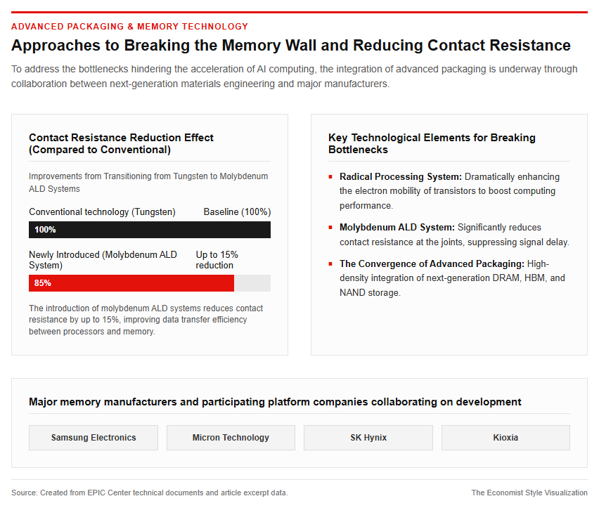
As back-end chip connection technology becomes the bottleneck determining AI performance, front-end thin-film deposition and etching technologies are being seamlessly combined with back-end die-to-wafer bonding technology to accelerate the mass production of power-efficient, high-bandwidth 3D integrated devices.
Impact on the Global Semiconductor Market and Geopolitical Risks
Acceleration of Cutting-Edge Process Development and Market Growth Forecast
The operation of the EPIC Center is expected to further boost the growth of the expanding AI semiconductor market. Applied Materials’ third-quarter revenue for fiscal 2026 reached $9.115 billion, a 25% increase year-over-year, setting a new all-time record for a single quarter. The company expects its semiconductor equipment business to grow by more than 20% in calendar year 2026, and specifically forecasts that revenue in the advanced packaging sector will record growth of over 70% in calendar year 2026. Please refer to the figure below for the market growth trends.
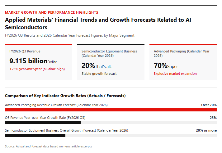
With predictions that total revenue in the global semiconductor market will reach the $1 trillion scale by 2026, capital investment appetite among cloud service providers remains extremely high. Through a joint development approach that incorporates customer requirements into equipment specifications from the early stages, semiconductor manufacturers can achieve higher yields and rapid fab startups, thereby maximizing investment efficiency.
Supply Chain Constraints and Compliance Management Challenges
While the market is growing rapidly, the semiconductor industry is facing a dual challenge: physical constraints on production capacity and tightening geopolitical regulations. The first constraint is the pace of cleanroom construction. Because completing a new fab takes three to four years, a situation exists where supply cannot keep up with demand in the short term. The second challenge is compliance with U.S. export control regulations. Applied Materials settled with the U.S. Department of Commerce’s Bureau of Industry and Security (BIS), receiving a near-record $252.5 million (approximately 38 billion to 39 billion yen) fine for improperly shipping ion implanters to China’s SMIC via its South Korean subsidiary between 2021 and 2022. Please refer to the figure below for the operational framework of regulatory compliance.
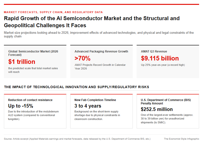
This case symbolizes the tightening of law enforcement against transshipments via third countries, making strict compliance management and transparency essential prerequisites for operating international joint development hubs.
Reference page
- [Applied Materials EPIC Center Official Page] https://www.appliedmaterials.com/jp/ja/epic.html
【#Semiconductors #AITechnology #SiliconValley #NextGenSemiconductors #JointDevelopment #AdvancedPackaging】

コメント