US-based GlobalFoundries has announced “FDX Fusion,” a next-generation FD-SOI platform that achieves 7nm-class digital performance. This announcement is driven by the soaring demand for power-efficient semiconductors in the field of physical AI, which requires real-time decision-making and control at the edge without relying on the cloud.
- Key Points of the FDX Fusion Announcement and Events
- 7nm-class digital performance and single-chip integration
- Cost Optimization Without FinFET or EUV
- Integration of STAC Features for Physical AI
- Reactions of Major Automotive and Robotics Companies
- Schedule for 2028 Mass Production, Future Developments, and Key Points to Watch
Key Points of the FDX Fusion Announcement and Events
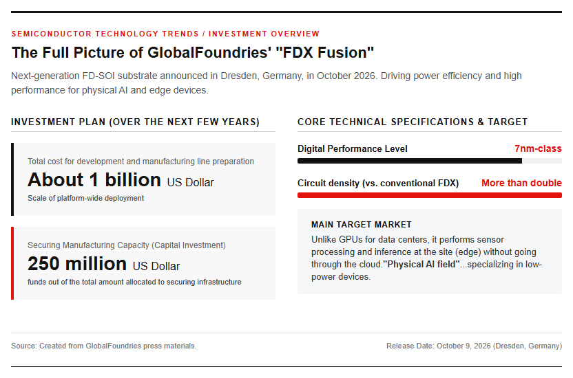
GlobalFoundries (GF), a major U.S. semiconductor foundry, announced its next-generation fully depleted silicon-on-insulator (FD-SOI) manufacturing technology, “FDX Fusion,” in Dresden, Germany, on October 9, 2026. Positioned as a direct evolution of the company’s conventional 22FDX platform, this technology is specifically designed for physical AI (artificial intelligence that operates in the real world). The company plans to invest approximately $1 billion in the development of this platform and the setup of production lines over the next few years, with $250 million of that amount allocated to capital expenditures aimed at securing manufacturing capacity. The first-generation manufacturing process is expected to achieve more than a twofold increase in circuit density compared to conventional FDX technology. Unlike massive power-consuming data center GPUs, it focuses on the edge AI device market, which handles sensor processing and inference locally in various terminals and industrial equipment. Please refer to the schematic diagram below.
With the full-scale adoption of this technology, reductions in processing latency and dramatic improvements in power efficiency are expected in edge computing environments.
7nm-class digital performance and single-chip integration
The greatest feature of FDX Fusion lies in its ability to achieve 7nm-class digital logic performance on a single chip while retaining the conventional planar structure. Going beyond mere advanced logic circuits, it integrates radio frequency (RF) circuits boasting a cutoff frequency (ft/fmax) of up to 0.5THz, high-precision analog mixed-signal functions, and ultra-low leakage current characteristics. Furthermore, embedded non-volatile memory (eNVM), in-memory computing (SRAM-based compute) functions, and high-density logic circuits (14 to 18 million gates per square millimeter) are integrated into the manufacturing platform. While conventional semiconductor design required the separate implementation of processing chips, communication chips, and memory, using this platform allows them to be densely and advancedly integrated. This makes it possible to dramatically reduce overall system complexity and board footprint, while resolving the challenges of power consumption and propagation delay caused by inter-chip interconnects.
Innovation in Manufacturing Processes and Optimization for Physical AI
Cost Optimization Without FinFET or EUV
In its technological manufacturing process, FDX Fusion does not adopt three-dimensional FinFETs, but instead continues to use FD-SOI with a thin-film structure featuring a silicon layer thickness of approximately 70 angstroms (7 nm). Its strength lies in its ability to suppress leakage current to the utmost limit through a fully depleted channel, gaining electrical advantages without forming Fin structures. Furthermore, it takes an approach that does not use extreme ultraviolet (EUV) lithography equipment, which is considered essential in cutting-edge 2nm and 3nm processes. While the latest FinFET processes require 70 to 80 exposure masks, FDX Fusion expects to reduce the number of masks to around 50. By combining advanced ArF immersion lithography and multi-electron-beam mask writing technology for the exposure technique, it achieves process simplification and yield improvement. By avoiding the enormous initial investment and operating costs of EUV lithography, it offers client companies an option with reduced development prototyping and manufacturing costs.
Integration of STAC Features for Physical AI
GlobalFoundries proposes a framework called “STAC (Sense, Think, Act, Communicate)” as a core set of capabilities required for physical AI. Devices that operate autonomously in the real world require not only the ability to perform massive computations, but also simultaneously demand sensor processing to recognize information from the external environment, actuator control to issue real-time control commands, and wireless communication capabilities to exchange data with their surroundings. Please refer to the functional configuration diagram below.
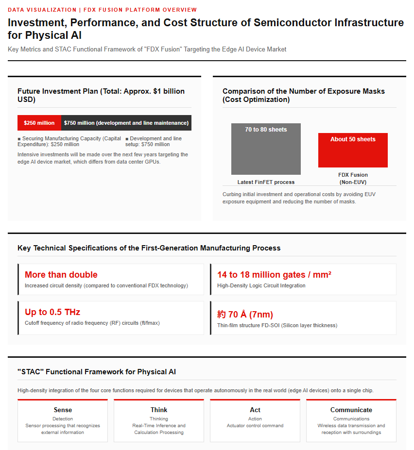
FDX Fusion is optimized to cover this entire STAC workload within a single semiconductor process. By leveraging a “body bias” function that dynamically adjusts the transistor threshold voltage by applying a voltage to the underside of the thin-film oxide, it achieves high-speed processing during operation while reducing leakage current in standby mode. This approach enables both dynamic power control and fast response, ranging from battery-powered mobile devices to robotics and autonomous driving systems.
Industry Evaluation and Future Manufacturing Roadmap
Reactions of Major Automotive and Robotics Companies
Following the announcement of FDX Fusion, strong expectations have been expressed by major automakers, industrial equipment vendors, and semiconductor manufacturers around the world. Germany’s Infineon Technologies is strengthening its partnership to jointly define and study 7nm-class FDX Fusion technology for next-generation millimeter-wave radar and wireless communication products. Additionally, Germany’s BMW Group and Bosch have highly evaluated the technology for its ability to power-efficiently integrate sensor input, AI inference, and real-time control in next-generation robotics and automotive control. Tesla of the US has also indicated that the company’s technology roadmap is extremely crucial for realizing edge-processing devices such as humanoid robots and autonomous driving systems. Furthermore, Germany’s Siemens and the Netherlands’ NXP Semiconductors have expressed their intent to validate the technology for application in industrial automation and highly reliable edge AI terminals, with initial development progressing toward early adoption across diverse fields.
Schedule for 2028 Mass Production, Future Developments, and Key Points to Watch
As part of its future roadmap, GlobalFoundries plans to provide proof-of-concept silicon chips for customer evaluation in early 2027, followed by the release of an initial Process Design Kit (PDK) in mid-2027. Subsequently, full-scale commercial volume production is scheduled to begin at its Dresden fab in Germany in 2028. The Dresden facility is undergoing an €1.1 billion expansion under the “SPRINT” project based on the European Chips Act, with plans to increase annual production capacity for 300mm wafers to over 1 million units by the end of 2028 through the addition of cleanroom space. Key points to watch include the timing of the final approval of public subsidies for the IPCEI AST project by the German government, as well as progress in developing the ecosystem for various IPs (such as processor cores and standard cells) accompanying the PDK release in 2027. Amid the ongoing social implementation of physical AI, establishing a mass production system for 7nm-class FD-SOI at a European manufacturing hub holds significant meaning in terms of global supply chain diversification and technological sovereignty.
Reference page
- 【GF unveils roadmap to deliver the world’s most advanced FD-SOI platform for Physical AI】https://gf.com/news-and-events/news/gf-unveils-roadmap-to-deliver-worlds-most-advanced-platform-for-physical-ai/
【#GlobalFoundries #FDSOI #FDXFusion #Semiconductors #PhysicalAI #EdgeAI】


コメント