The Prefectural University of Kumamoto has announced plans to establish Japan’s first-ever School of Semiconductors in April 2027. This groundbreaking initiative comes in response to TSMC’s major expansion into Kumamoto and the subsequent, critical shortage of specialized semiconductor talent.
- Inside the Prefectural University of Kumamoto’s Semiconductor Initiative
- A Powerhouse Faculty: World-Class Researchers and Industry Pioneers
- Multi-Disciplinary Tracks Designed to Tackle Real-World Challenges
- Bridging the Semiconductor Talent Gap: The Kumamoto Advantage
- Empowering Local Youth to Drive Regional Revitalization
- Spearheading a National Shift in Technology and Education
Inside the Prefectural University of Kumamoto’s Semiconductor Initiative
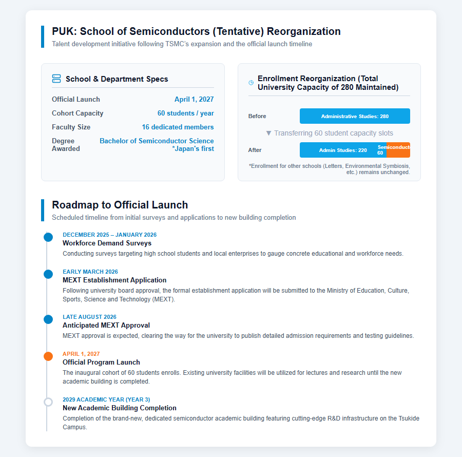
On September 22, 2025, the Prefectural University of Kumamoto (PUK) and the Kumamoto Prefectural Government held a joint press conference to officially unveil their plan to establish a School of Semiconductors, Department of Semiconductors (tentative name). The press conference featured Kumamoto Governor Takashi Kimura, PUK Board Chairperson Tadahiro Kuroda, and PUK President Hiroaki Tsutsumi, who outlined the vision and structure of this pioneering school. Scheduled to open on April 1, 2027, the school will welcome 60 students per cohort under the guidance of 16 dedicated faculty members. While PUK’s overall annual enrollment capacity of 280 will remain unchanged, the university will shift resources by reducing the capacity of its existing School of Administrative Studies from 280 to 220. Graduates will be awarded Japan’s first-ever Bachelor of Semiconductor Science degree. The university plans to construct a state-of-the-art academic building at its Tsukide Campus by the 2029 academic year, which marks the third year of the program. Until then, existing facilities will be leveraged to facilitate classes and research. Governor Kimura expressed high expectations, stating that the new school will address the region’s acute talent shortage and serve as a cornerstone for Kumamoto’s long-term economic growth and technological innovation.
A Powerhouse Faculty: World-Class Researchers and Industry Pioneers
To guarantee top-tier education and research, PUK has assembled an exceptionally distinguished faculty of global academic authorities and industry veterans. Dr. Hideharu Amano, Professor Emeritus at Keio University and a leading expert in computer architecture who has mentored 200 students over a 40-year career, is slated to become the Dean. The Department Chair position will be filled by Dr. Masaaki Niwa, a former professor at Tohoku University with extensive R&D experience at Panasonic, who previously led next-generation semiconductor development at premier international research institutions. PUK Board Chairperson Tadahiro Kuroda—himself a Tokyo University Special Professor and a world-renowned authority in semiconductor design—will also teach, providing students with an incredibly rare opportunity to learn directly from top global scholars in a highly supportive, low-student-to-faculty environment. Regarding the timeline, PUK will run surveys targeting high school students and local enterprises from December 2025 through January 2026 to gauge educational and workforce demands. Following board approval, PUK intends to submit its formal establishment application to the Ministry of Education, Culture, Sports, Science and Technology (MEXT) in early March 2026. If all goes smoothly, MEXT approval is anticipated by late August 2026, clearing the way for the school’s 2027 debut. Please refer to the official press conference document below.
A Forward-Looking Curriculum Grounded in Japan’s “Silicon Island”
Multi-Disciplinary Tracks Designed to Tackle Real-World Challenges
Rather than focusing solely on fabrication, the School of Semiconductors aims to cultivate tech-savvy generalists capable of leveraging semiconductor technology to solve complex societal problems. To achieve this, the curriculum offers three specialized learning tracks. The AI and Advanced Information track dives into application areas driven by artificial intelligence, covering image processing, robotics, and signal processing. The Microelectronics track focuses on the core of semiconductor design, covering LSI design, analog integrated circuits, power control, and wireless communications. Finally, the Smart Materials track equips students with advanced knowledge of device physics, nanotechnology, 3D integration, and the manufacturing equipment and materials required to build modern chips. Students will acquire a comprehensive foundation in semiconductor science through the first half of their third year, before choosing a laboratory to conduct their fourth-year graduation research. Chairman Kuroda stresses that as Artificial General Intelligence (AGI) moves toward widespread social integration around 2030—automating transportation, healthcare, and logistics—the world will desperately need professionals who understand massive datasets and can effectively guide technology to fit human and social needs.
Bridging the Semiconductor Talent Gap: The Kumamoto Advantage
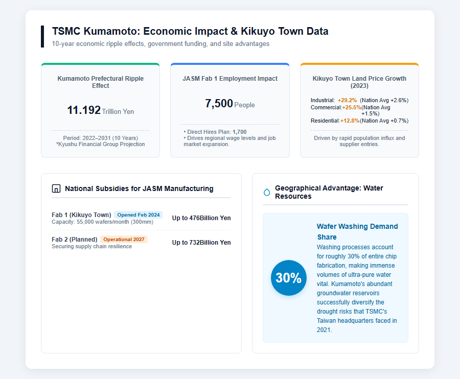
This historic initiative is directly driven by Taiwan Semiconductor Manufacturing Company (TSMC)—the world’s premier dedicated semiconductor foundry—and its decision to build a manufacturing hub in Kikuyo Town, Kumamoto. Setting up Japan Advanced Semiconductor Manufacturing (JASM) as a joint venture with Sony Semiconductor Solutions and Denso, TSMC officially inaugurated its first plant on February 24, 2024. This initial factory alone is bringing 1,700 direct jobs, with the total regional employment impact estimated to reach 7,500 positions. According to projections by the Kyushu Financial Group, the economic ripple effect in Kumamoto Prefecture is expected to reach a staggering 11.192 trillion yen over the ten-year period from 2022 to 2031. Kyushu has long been dubbed “Silicon Island” due to its dense cluster of approximately 1,000 semiconductor-related businesses, making material sourcing and supply-chain logistics exceptionally efficient. Crucially, Kumamoto’s natural environment offers a decisive advantage. Chip fabrication requires immense volumes of ultra-pure water, with washing steps accounting for roughly 30% of the entire process. Kumamoto’s vast, pristine groundwater reservoirs offer a highly stable supply, mitigating the severe drought risks that TSMC’s headquarters in Taiwan experienced in 2021. The diagram below illustrates the economic and operational landscape of Kumamoto’s semiconductor industry.
The Vital Role of Public Universities in Shaping Japan’s Industrial Future
Empowering Local Youth to Drive Regional Revitalization
PUK is deliberately focusing on attracting high school students from Kumamoto and broader Kyushu, a strategy reflecting its commitment to long-term community sustainability. While many engineers currently working at Kumamoto’s newly established facilities have relocated from other prefectures, relying on transient or solo-commuting personnel is unsustainable for building a deeply rooted local ecosystem. PUK’s vision is to establish a virtuous loop where local talents study, work, and compete globally without having to leave their hometowns. Furthermore, modern chip fabrication is highly automated; human roles have shifted from manual labor to intellectually engaging tasks such as data analysis, AI control, and cybersecurity. As a university with historical roots as a women’s college and a high female enrollment rate, PUK sees the semiconductor sector as a prime field for female career advancement. Public tuition rates offer another massive advantage. Admission fees are exceptionally low—approximately 210,000 yen for prefecture residents and 420,000 yen for out-of-prefecture students—and annual tuition is roughly 540,000 yen. This is less than half the cost of private science and engineering programs, making elite tech education affordable and accessible to all.
Spearheading a National Shift in Technology and Education
After slipping from its 1980s golden age, Japan’s semiconductor sector now faces severe labor shortages and intense global competition. In response, the Japanese government has designated semiconductors as a “specified critical material,” backing TSMC’s first plant with up to 476 billion yen and the planned second plant with up to 732 billion yen. Simultaneously, MEXT is deploying its University and KOSEN Function Enhancement Support Project (a fund for transitioning to growth fields) to aggressively support the restructuring of academic departments and the creation of public technical colleges across Japan. PUK’s School of Semiconductors is a key beneficiary of this national funding. Similar restructuring efforts are gaining momentum nationwide to meet regional industry needs, including the University of Kitakyushu’s planned School of Information Innovation in 2027 and the Prefectural University of Hiroshima’s new data-focused initiatives. With Japan’s university-bound population projected to plunge to around 460,000 by 2040, breaking down the traditional barrier between humanities and sciences is crucial. Continually nurturing highly skilled, tech-literate professionals within local regions will be the ultimate key to establishing a resilient economy and securing Japan’s status as a leading technology nation.
References
- 【School of Semiconductors (Tentative Name) Special Site | Prefectural University of Kumamoto】https://semi.pu-kumamoto.ac.jp/
- 【Joint Press Conference on Semiconductor Talent Development at the Prefectural University of Kumamoto | Kumamoto Prefectural Government Website】https://www.pref.kumamoto.jp/soshiki/8/246779.html
【#Semiconductors #PrefecturalUniversityOfKumamoto #TSMC #CollegeAdmissions #RegionalRevitalization #ScienceAndTechnology】


コメント