
Rapidus has announced “Rapidus CORE,” an ecosystem designed to support the development and mass production of cutting-edge semiconductors, and has initiated partnerships with 17 companies in Japan and overseas as its first wave of collaboration. Aiming for the mass production of 2nm logic semiconductors in the second half of fiscal 2027, the move is intended to unearth latent demand by providing comprehensive, end-to-end support for customers ranging from design to manufacturing.
- Key Takeaways: Launch of the “Rapidus CORE” Ecosystem and the Full Scope of the 17-Company Collaboration
- Background of the Collaboration: Overcoming Design Walls and Talent Shortages in the 2nm Generation
- Complementary structure of roles and specialized fields among 17 companies
- Chances of Winning as a Latecomer: Confronting TSMC and Speed & Pricing Strategies
- Public-Private Financing and Public Support: A Cumulative ¥3 Trillion Investment Structure
- Future Outlook and Key Points: Roadmap to 2027 Mass Production and Customer Acquisition
Key Takeaways: Launch of the “Rapidus CORE” Ecosystem and the Full Scope of the 17-Company Collaboration
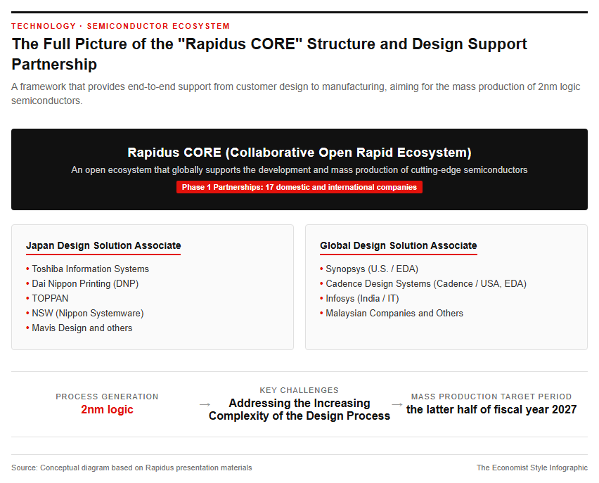
On October 5, 2026, Rapidus, aiming for the domestic production of next-generation semiconductors, announced the launch of “Rapidus CORE (Collaborative Open Rapid Ecosystem),” a global ecosystem to support the development and mass production of cutting-edge semiconductors, and selected 17 domestic and international companies as “Design Solution Associates” as its initial phase. The partner companies include domestic firms such as Toshiba Information Systems (a subsidiary of Toshiba), Dai Nippon Printing, TOPPAN, NSW, and Mavis Design, alongside major global Electronic Design Automation (EDA) giants such as US-based Synopsys and Cadence Design Systems, Indian IT services giant Infosys, and Malaysian companies. In the development of cutting-edge logic semiconductors for the 2nm (nanometer) circuit linewidth generation, processes ranging from logic design to physical design, structural design, and verification are becoming significantly complex. By not only providing its own contract manufacturing capabilities (foundry) but also jointly building an environment with external specialized companies that allows customers to smoothly design and develop chips, Rapidus is rapidly accelerating customer acquisition toward the start of mass production scheduled for the second half of fiscal 2027. The following image is a conceptual diagram of the design collaboration.
Background of the Collaboration: Overcoming Design Walls and Talent Shortages in the 2nm Generation
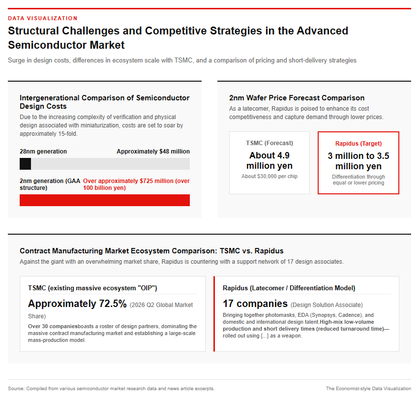
In the development of cutting-edge 2nm-process semiconductors, the biggest barriers are the soaring cost of design and a shortage of specialized talent. According to semiconductor market research data, while the design cost for the 28nm generation was approximately $48 million, it is estimated to skyrocket to approximately $725 million (over 100 billion yen) for the 2nm generation. Integrating tens of billions of transistors and controlling a three-dimensional structure known as a GAA (gate-all-around) architecture requires advanced verification and complex physical design. However, due to delays in horizontal specialization over the past 30 years in Japan, there has been a severe shortage of advanced semiconductor design engineers, leading to the challenge where automotive and industrial equipment manufacturers considering the development of their own custom chips are unable to complete designs on their own. For Rapidus, to avoid the risk of running a fab without customers, it was essential to bring together external design firms and EDA vendors to systematically make up for the “design capabilities of the ordering side.” This partnership establishes a framework enabling even customers with only logic design know-how to smoothly hand off production by utilizing partner companies and Rapidus’s PDK (Process Design Kit).
Battles with Global Competitors and Business Strategy
Complementary structure of roles and specialized fields among 17 companies
The 17 Design Solution Associates selected this time play mutually complementary roles in the semiconductor design value chain. Dai Nippon Printing and TOPPAN have strengths in photomask manufacturing for transferring circuit patterns and are well-versed in the handover from design data to the manufacturing process. In addition, design service companies such as Toshiba Information Systems, NSW, and MVIS Design have a wealth of track records in embedded system design for automotive and industrial equipment, handling everything from listening to customer specifications to actual chip design on their behalf. Furthermore, the participation of Synopsys and Cadence, which divide the EDA market between them, will advance the sharing of cutting-edge AI-powered automated design tools and IP (intellectual property). In addition, by incorporating companies with abundant overseas design human resources, such as Infosys and Malaysian firms, a structure has been completed that compensates for the domestic labor shortage with global resources. The 17 companies will not only execute design operations on behalf of customers, but will also function as sales contact points (bridges) to introduce Rapidus’ contract manufacturing services to their own existing customers, making them powerful channels for Rapidus to discover projects around the world.
Chances of Winning as a Latecomer: Confronting TSMC and Speed & Pricing Strategies
In the contract manufacturing market, Taiwan’s TSMC holds a global market share of approximately 72.5% (as of the second quarter of 2026) and dominates the market by building a massive ecosystem called “OIP” with over 30 design partners. Since it is difficult for latecomer Rapidus to compete head-on using the same mass-production model, the company has deployed a differentiation strategy with high-mix low-volume production and short delivery times (reduced turnaround times) as its greatest strengths. While aiming to cut manufacturing time in half by introducing single-wafer processing lines that process wafers one by one, President Atsuyoshi Koike has announced a policy to set the selling price of 2nm semiconductors “equal to or lower than TSMC.” While TSMC’s 2nm wafer price is projected to be around $30,000 (approx. 4.9 million yen) per wafer, Rapidus is targeting around 3 million to 3.5 million yen per wafer to enhance its cost competitiveness. In addition to Fujitsu’s decision to outsource the production of its AI processors, negotiations are underway with over 60 potential customers, including Tenstorrent in the U.S. and IBM Japan, positioning the company to capture demand for application-specific custom chips through a combination of its design support network, short delivery times, and low pricing. The figure below shows a comparison of the ecosystem with TSMC.
Frameworks for National Support and Future Prospects
Public-Private Financing and Public Support: A Cumulative ¥3 Trillion Investment Structure
Rapidus’s project is positioned as a critical national initiative supporting Japan’s economic security. In February 2026, the company raised a total of approximately 267.6 billion yen from both the public and private sectors. Through the IPA (Information-technology Promotion Agency), the government contributed about 100 billion yen, while 32 private companies, including Toyota Motor, NTT, SoftBank, Sony Group, and Fujitsu, invested a combined 167.6 billion yen. Cumulative subsidies and investments by the Ministry of Economy, Trade and Industry have already reached the scale of 2.3 trillion to 2.6 trillion yen, with total support of around 3 trillion yen planned by the start of mass production. Against the backdrop of an estimated 4 trillion to 7 trillion yen in total investment required for the entire project, public-private fundraising is progressing, with Japan’s three mega-banks, including MUFG Bank, considering loans of up to 2 trillion yen backed by government guarantees. Meanwhile, accompanied by the expansion of government investment, the government will hold an 11.5% voting stake and veto power (golden shares), and a framework is being established that would allow it to acquire management control in an emergency, strengthening its aspect as a “national policy company.” Moving forward, there is a strong demand to break away from subsidy dependency and establish independent cash flow through contract manufacturing.
Future Outlook and Key Points: Roadmap to 2027 Mass Production and Customer Acquisition
The biggest focus moving forward will be whether it can secure firm volume orders (anchor customers) for the full-scale mass production of 2nm semiconductors at the “IIM-1” plant in Chitose, Hokkaido, scheduled for the latter half of fiscal 2027. Rapidus has steadily achieved technical milestones, such as launching its front-end pilot line in April 2025, successfully verifying the operation of 2nm GAA transistors in July of the same year, and launching its back-end (chiplet and 3D packaging) line in April 2026. However, semiconductor fabrication plants have a business structure that results in losses due to massive fixed costs unless high utilization rates are maintained. Whether the recently announced collaboration with 17 companies goes beyond mere partnership announcements and translates into actual tape-outs (design completion) and mass-production outsourcing contracts will determine the business’s independence. Key indicators that investors and industry insiders should watch going forward include the progress of additional private fund-raising, the expansion of EDA and IP partners, the development roadmap for the 1.4nm generation, and the disclosure of specific mass-production contracts with major domestic and international AI and automotive manufacturers. It remains to be seen whether the design collaboration with 17 companies, including Toshiba, will yield results and establish a foundation that enables Japan’s manufacturing industry to utilize advanced semiconductors.
Reference Page
- [Rapidus Corporation Official Announcement] https://www.rapidus.inc/news_topics/news-info/20261005-2/
- 【Ministry of Economy, Trade and Industry: Information Related to Next-Generation Semiconductors, etc.】https://www.meti.go.jp/
【#Rapidus #Semiconductors #2nmMassProduction #RapidusCORE #METI #SemiconductorDesign】


コメント