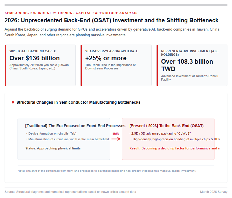
Driven by the rapid surge in demand for AI semiconductors, it has been revealed that semiconductor back-end (OSAT) companies in Taiwan, China, South Korea, Japan, and other regions will make massive capital expenditures totaling over $136 billion (approx. 20 trillion yen) in 2026. This is driven by the bottleneck shifting from front-end processes to 2.5D/3D advanced packaging “CoWoS,” as seen in moves such as back-end leader ASE Holdings advancing an investment of over NT$108.3 billion at its Renwu facility in Taiwan.
- Key Points of the Event: The Background Behind the 6 Billion Back-End Investment Set to Move in 2026
- Investment Trends of Major OSATs: ASE Holdings’ NT8.3 Billion Large-Scale Facility Construction
- Advanced Packaging Supply Crunch and TSMC’s Expansion of CoW Process Outsourcing
- The “Hidden Wall” of Cascading Parts and Materials Shortages and a Surge in Inspection Times
- Mass Production of Co-Packaged Optics (CPO) and Transition to Next-Generation Technologies
- Accelerating Base Dispersion and New Business Opportunities Spreading Among Japanese Companies
Key Points of the Event: The Background Behind the 6 Billion Back-End Investment Set to Move in 2026
According to a March 2026 survey, semiconductor back-end processing companies in Taiwan, China, South Korea, Japan, and other regions are planning unprecedented capital expenditures totaling more than $136 billion (approximately 20 trillion yen) during 2026. This scale of investment represents a massive year-over-year increase of over 25%, indicating that the importance of back-end processing in the semiconductor industry is rapidly growing. This trend is driven by the explosive surge in demand for graphics processing units (GPUs) and accelerators accompanying the rise of generative AI. Traditionally, large-scale capital investment in the semiconductor industry was concentrated on “front-end” fabrication (fabs) to form elements on circuits. However, as the miniaturization of circuit linewidths approaches its physical limits, “back-end” packaging technology—which bonds multiple chips and high-bandwidth memory (HBM) onto a single substrate with high density and precision—has become a decisive factor dictating overall chip performance and shipment volumes. The following figure illustrates the global investment expansion in back-end processing.
As a result, the production capacity of outsourced semiconductor assembly and test (OSAT) companies has become extremely tight, with their lines completely filled with orders from major AI semiconductor makers like NVIDIA. A severe supply shortage has forced them to turn down orders from small and medium-sized customers, prompting OSAT companies to aggressively acquire existing cleanrooms and build new plants at a furious pace.
Investment Trends of Major OSATs: ASE Holdings’ NT8.3 Billion Large-Scale Facility Construction
Taiwan’s ASE Holdings, which boasts the world’s top market share in the back-end market, has unveiled the largest-ever investment plan in its history for 2026. The company has decided to begin the construction and expansion of new plants across six locations worldwide in 2026, announcing a plan to invest over NT$108.3 billion (approx. 500 billion yen) at the Renwu site in Kaohsiung, Taiwan alone. At the Renwu site, the Phase 1 plant is expected to begin operations in April 2027, and the Phase 2 plant in October of the same year. In addition to this, the company held a groundbreaking ceremony in March 2026 for two new plants with an investment of NT$17.8 billion (approx. 89 billion yen) in Phase 3 of the Nanzih Technology Industrial Park in Kaohsiung, which aims to start operations in the second quarter of 2028. ASE’s annual capital expenditure (CapEx) budget for 2026, initially set at $7 billion, is highly likely to be revised upward driven by strong customer demand. This investment rush by OSAT companies is not limited to Taiwan. Amkor Technology of the U.S., SPIL (Siliconware Precision Industries) of Taiwan, and Powertech Technology are also pursuing large-scale capacity enhancements. Furthermore, Micron Technology of the U.S. has opened a back-end plant for memory totaling $2.75 billion (approx. 434 billion yen) utilizing government subsidies in Gujarat state in western India, and will begin assembling tens of millions of chips within 2026, expanding the back-end supply chain on a global scale.
Why the “Back-End” is Now the Main Battleground in the Semiconductor Supply Chain
Advanced Packaging Supply Crunch and TSMC’s Expansion of CoW Process Outsourcing
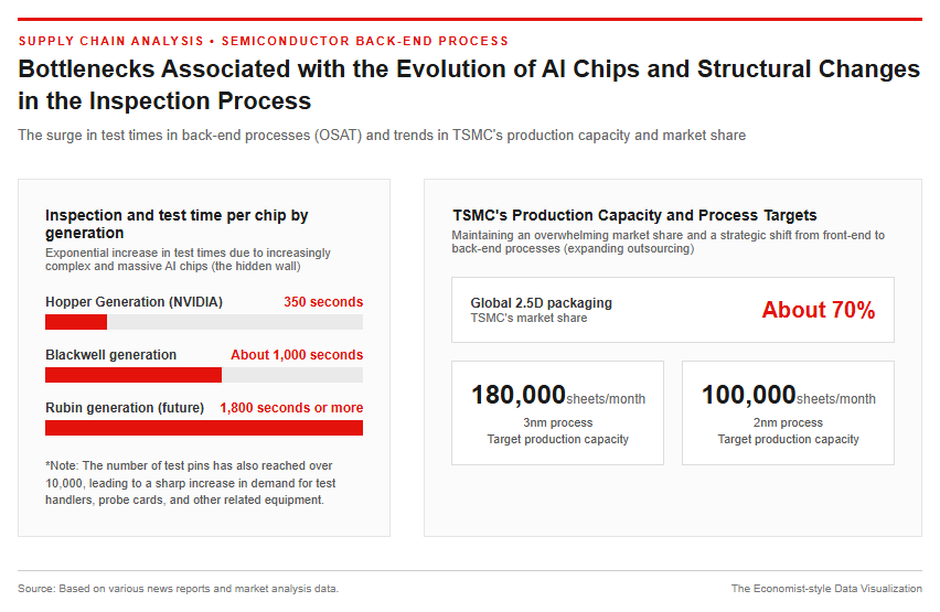
The biggest factor behind the surge in investment in back-end processes is the extreme supply shortage of “CoWoS (Chip on Wafer on Substrate),” a 2.5D advanced packaging technology deployed by Taiwan Semiconductor Manufacturing Company (TSMC). CoWoS is a technology that closely places logic chips, such as GPUs, in the center and surrounding HBM on a silicon interposer, and is considered essential for the manufacturing of AI accelerators. TSMC holds an overwhelming share of around 70% of the world’s 2.5D packaging capacity, but a severe bottleneck where production cannot keep up with demand has continued for three consecutive years since 2023. To resolve this bottleneck, TSMC has made a major strategic shift. Up until now, TSMC has mainly outsourced the “WoS (Wafer on Substrate)” process—which bonds the interposer to the main board—to external parties, while keeping the “CoW (Chip on Wafer)” process of placing chips on the interposer in-house. However, to cope with expanding demand from NVIDIA, AMD, Broadcom, and others, TSMC has decided to expand the outsourcing of additional CoW capacity to major OSATs such as ASE. As a result, various OSAT companies are placing large-scale orders for equipment such as bonders and laser processing systems to set up cutting-edge CoW contracted processing facilities. TSMC is rapidly proceeding with the ramp-up of its 2nm process (targeting 100,000 wafers per month) and 3nm process (targeting 180,000 wafers per month) in its front-end operations, adopting a strategy to maintain overall shipment speeds by jointly boosting back-end production capacity with external OSATs.
The “Hidden Wall” of Cascading Parts and Materials Shortages and a Surge in Inspection Times
Supply constraints in the back-end process are not limited simply to the floor space of packaging plants and assembly equipment; they extend to upstream and downstream components and the entire inspection process. In addition to wafer-on-substrate (WoS) technology, ABF substrates, printed circuit boards (PCBs), and high-performance copper-clad laminates (CCLs)—all of which are essential for advanced packaging—the supply of stacked HBM and SSDs is also severely congested. According to an analysis by Nomura Securities, it has been pointed out that from the second half of 2026 through 2027, the WoS process and related components could become an even greater supply bottleneck than CoWoS itself.
Furthermore, another “hidden wall” in the back-end process is the explosive increase in chip inspection and testing time. As AI chips become more complex and massive, the test time per chip is surging rapidly—from 350 seconds for NVIDIA’s Hopper generation to approximately 1,000 seconds for the Blackwell generation, and over 1,800 seconds for the future Rubin generation. Because the number of test pins also reaches over 10,000, the required volume of testing equipment and consumables, such as test handlers, probe cards, and test sockets, is increasing exponentially. The importance of specialized testing and equipment manufacturers such as King Yuan Electronics (KYEC) and Hon Precision is growing, making the testing process itself a factor that dictates the operating rates of the back-end process.
Future Outlook and Impact on Industries Under Geopolitical Risks
Mass Production of Co-Packaged Optics (CPO) and Transition to Next-Generation Technologies
The biggest point of interest in the future back-end market is the full-scale implementation of “Co-Packaged Optics” (CPO) and silicon photonics technologies, which are shifting course from conventional metal wiring (telecommunications) to optical connections. As data transmission volumes in AI servers surge rapidly, conventional copper wiring faces severe barriers such as bandwidth limitations and increases in heat generation and power consumption. CPO is a next-generation technology that drastically reduces power consumption and achieves ultra-high-speed transmission by mounting LSI chips and optical engines in close proximity within the same package. ASE Holdings has explicitly stated that it will begin initial mass production of CPO as early as 2026, demonstrating that back-end technology has stepped into the realm of optoelectronic convergence. The following figure illustrates the layout structure of next-generation optoelectronic convergence packaging.
Going forward, the standardization of CPO and the establishment of an optical module ecosystem will hold the key to adoption. Furthermore, options for alternative packaging technologies to TSMC’s dominance with CoWoS are expanding—such as Intel’s adoption of EMIB (Embedded Multi-die Interconnect Bridge) and glass substrate technology—and the technological system of advanced backend processes is expected to become increasingly multi-layered.
Accelerating Base Dispersion and New Business Opportunities Spreading Among Japanese Companies
Driven by concerns over geopolitical risks, a gradual decentralization of manufacturing hubs from Taiwan—a major cluster for semiconductor production—to various parts of the world is underway. Paralleling TSMC’s expansion into Arizona (USA), Kumamoto (Japan, via JASM), and Dresden (Germany), multi-source procurement to mitigate geopolitical risks is also becoming common in the back-end process. This tectonic shift presents the largest business opportunity in history for Japanese companies possessing advanced technological capabilities. In the semiconductor back-end process, a wide variety of Japanese materials and equipment manufacturers play indispensable roles, ranging from ultrapure water supply, high-purity chemicals, and encapsulation resin materials to dicing and bonding equipment, high-precision inspection systems, and even cleanroom construction (EPC). Domestically, the reconstruction of the domestic supply chain is accelerating not only in the front-end but also in the back-end processes; for instance, the “Japan OSAT Association,” which aims to improve back-end technologies through industry-academia collaboration, has established an office within Kumamoto University. Although supply and demand tightness in the back-end process is expected to gradually level off from 2026 to 2028, high levels of investment are projected to continue driven by the expansion of AI inference demand and the rise of robotics, making the restructuring of the global supply chain centered on the back-end process a development that cannot be ignored.
Reference Page
- [Institute of Developing Economies] Taiwan as the World’s Semiconductor Factory and Geopolitical Risks — From Concentration to Gradual Dispersion
 The requested page was not found. - Institute of Developing EconomiesThe Institute of Developing Economies (IDE) aims to make intellectual contributions to the world as a leading center of ...www.ide.go.jp
【#Semiconductor #AISemiconductors #OSAT #AdvancedPackaging #CoWoS #TSMC #CapitalInvestment #SupplyChain】
コメント