
Oji Holdings has developed a PFAS-free, next-generation semiconductor photoresist derived from wood biomass, successfully forming ultra-fine patterns in cutting-edge EUV lithography. This breakthrough is driven by growing demand for PFAS alternatives due to environmental regulations and the accelerating transition toward a decarbonized society.
- Key Breakthroughs Announced by Oji Holdings
- Technological Context: High-NA EUV Lithography and the A14 Generation
- Breakthrough Driven by Joint Research with Global Institute imec
- Stricter Global PFAS Regulations and Semiconductor Industry Challenges
- Advantages of Biomass-Derived Materials Free from Hazardous Chemicals
- Future Outlook: Target Commercialization in 2028 and Key Milestones
Key Breakthroughs Announced by Oji Holdings
Oji Holdings Corporation announced on September 4, 2026, that it demonstrated exceptionally high resolution performance in semiconductor photoresists (“biomass resists”) derived primarily from wood biomass resources, adapted for state-of-the-art semiconductor manufacturing technology. Specifically, using high-numerical-aperture (High-NA, NA=0.55) extreme ultraviolet (EUV) lithography evaluation, the company confirmed the formation of fine patterns required for advanced node processes. It successfully achieved a 10 nm (nanometer) line-and-space pattern and 16 nm diameter contact hole patterns. This marks the world’s first demonstration of potential applicability to the “A14 generation” (equivalent to the 1.4 nm node), targeted for mass production in 2028 and beyond. Bringing together its deep expertise in impurity removal and purification of wood polymers cultivated through its paper manufacturing heritage, Oji Holdings has created a revolutionary semiconductor material that does not rely on traditional petroleum-derived chemicals. The figure below illustrates visual observations of fine patterns formed by the biomass resist and the conceptual overview of this development.
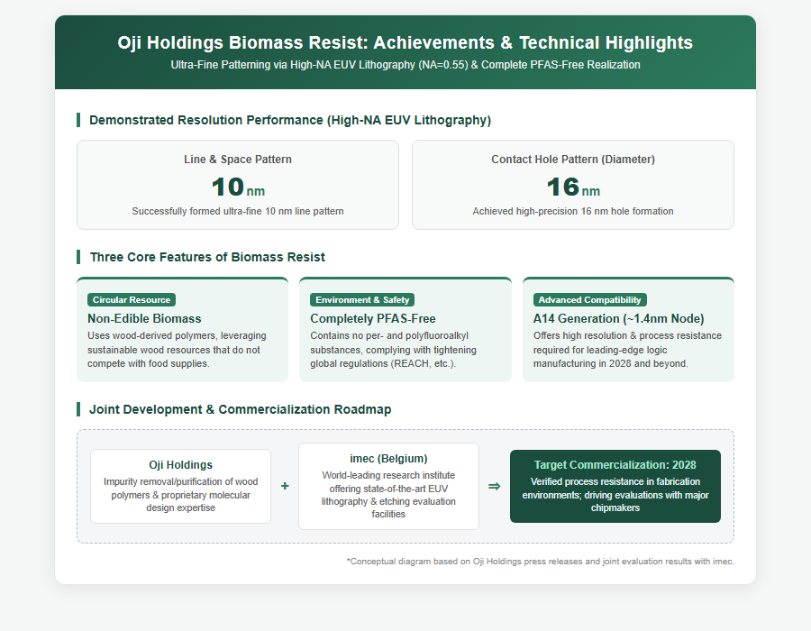
Key characteristics of the developed biomass resist include:
– Utilization of non-edible wood biomass raw materials, avoiding competition with food supplies while leveraging circular resources.
– A completely PFAS-free design containing no per- and polyfluoroalkyl substances, which are known for environmental and health hazards.
– High thermal and process stability coupled with resolution performance exceeding that of conventional petroleum-derived photoresists.
Technological Context: High-NA EUV Lithography and the A14 Generation
In driving higher performance and lower power consumption in semiconductors, further miniaturization of circuit patterns remains essential. Demand for cutting-edge chips is surging, particularly for AI servers, data centers, and high-performance computing (HPC). As a result, manufacturing processes are transitioning beyond the 2 nm node toward the A14 generation (1.4 nm class). The A14 generation represents the benchmark for leading-edge logic semiconductor manufacturing expected from 2028 onward, demanding unprecedented precision in circuit formation.
The key to enabling this ultra-miniaturization is High-NA EUV lithography. By increasing the numerical aperture of the optical lens system to 0.55—compared to 0.33 in conventional EUV equipment—light resolution is significantly improved, allowing much finer circuits to be printed. However, as light wavelengths shrink and features become extremely small, photoresist materials face stringent performance demands. They require precise photo-reactivity and film uniformity to prevent resolution degradation or line distortion under extreme light exposure. By meticulously controlling the molecular structure of wood-derived polymers, Oji Holdings’ biomass resist satisfied the rigorous exposure conditions of High-NA EUV equipment, achieving 10 nm line patterning.
Breakthrough Driven by Joint Research with Global Institute imec
This landmark technical demonstration was accomplished through joint research with imec, a world-leading semiconductor research institute headquartered in Belgium. In 2024, Oji Holdings developed the foundational technology for EUV-compatible biomass resists. In 2025, the company joined imec’s joint development platform dedicated to advanced lithography technology. Within imec’s testing environment, where major global semiconductor manufacturers, equipment vendors, and material suppliers collaborate, extensive evaluations were conducted using state-of-the-art EUV lithography and etching tools under conditions mimicking actual production lines.
Through this collaborative evaluation process, the biomass resist demonstrated superior process resistance capable of withstanding lithography and subsequent etching operations in front-end semiconductor manufacturing. For a materials manufacturer to prove commercial-grade performance in a global, top-tier research platform beyond its internal laboratories marks a crucial milestone in establishing industry trust. The synergy between Oji Holdings’ cellulose purification expertise from papermaking and world-leading semiconductor evaluation infrastructure opened a clear path to creating innovative high-tech materials from forest resources.
Heightened PFAS Regulations and the Impact of Sustainable Material Transition
Stricter Global PFAS Regulations and Semiconductor Industry Challenges
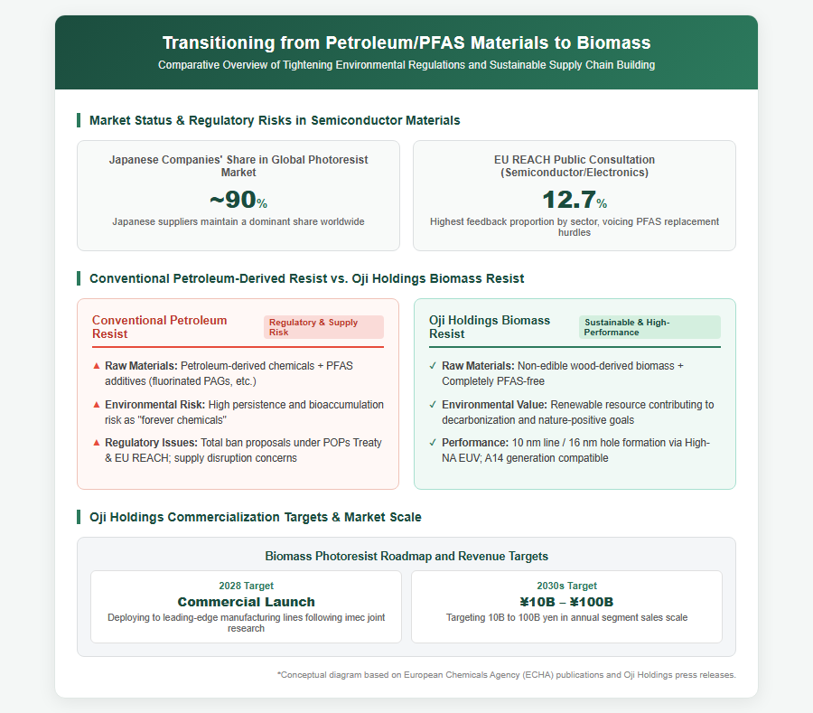
Global regulations targeting PFAS (per- and polyfluoroalkyl substances) are tightening rapidly. Due to their exceptional heat resistance, water/oil repellency, and chemical stability, PFAS have been widely used across semiconductor fabrication—including lithography, dry etching, cleaning solutions, and equipment piping components. However, because they resist natural degradation and pose risks of persistent environmental and bioaccumulative contamination as “forever chemicals,” global efforts under the POPs Convention and European REACH regulations are pushing toward comprehensive bans.
In a public consultation conducted by the European Chemicals Agency (ECHA) regarding proposed REACH restrictions, the electronics and semiconductor sector submitted the highest proportion of feedback at 12.7%. The semiconductor industry raised strong concerns that “no functional equivalents currently exist, and immediate blanket bans would risk shutting down production lines.” When legacy compounds such as PFOS and PFOA were previously phased out, replacing them required many years—and most alternatives were themselves other forms of PFAS. Thus, comprehensive PFAS restrictions present an existential challenge to the industry.
Advantages of Biomass-Derived Materials Free from Hazardous Chemicals
In response to severe supply chain risks and environmental mandates, Oji Holdings’ biomass resist offers a fundamental solution. Traditional semiconductor photoresists heavily rely on PFAS-based additives and photoacid generators (PAGs) to maintain sensitivity and resolution during exposure. In contrast, Oji Holdings designed its resist around proprietary molecular engineering of non-edible wood-derived polymers, attaining high resolution without adding PFAS or other hazardous additives.
Adopting biomass photoresists not only mitigates regulatory risks but also substantially reduces environmental impact across the product lifecycle, advancing decarbonization and nature-positive goals. Although Japanese chemical suppliers hold approximately 90% of the global photoresist market, environmental compatibility is quickly becoming a critical competitive factor alongside resolution performance. Grounded in renewable wood resources, this technology enables a sustainable semiconductor supply chain combining raw material security with environmental safety. The figure below compares conventional chemical materials with the transition to biomass-derived alternatives.
Future Outlook: Target Commercialization in 2028 and Key Milestones
Building on these verified results, Oji Holdings plans to advance customer evaluations and technology optimization, targeting commercialization in 2028. The semiconductor photoresist market is projected to expand significantly from 2024 through 2030, propelled by advancements in AI technology and automotive electronics. Oji Holdings aims for related business sales of 10 billion to 100 billion yen in the 2030s. Moving forward, key priorities include strengthening partnerships with research institutes like imec and leading semiconductor chipmakers, while establishing mass-production quality assurance frameworks and refining process compatibility.
This initiative—repurposing forest resources and wood biomass technologies cultivated in traditional papermaking for cutting-edge semiconductors—symbolizes the transformation of a mature materials manufacturer into a high-value tech innovator. Amid declining graphic paper demand, Oji Holdings is accelerating its portfolio shift toward multi-faceted biochemical businesses, including bioethanol, polylactic acid (PLA) bioplastics, and wood-derived pharmaceuticals. Successful commercial implementation of biomass resists in ultra-fine semiconductor fabrication promises a major breakthrough, positioning Japanese materials technology to lead both global decarbonization and the sustainable evolution of the semiconductor industry.
Reference Pages
- 【Oji Holdings Corporation Corporate Website】https://www.ojiholdings.co.jp/
- 【Oji Holdings Innovation Promotion Division】https://www.oji-rd.jp/
【#OjiHoldings #PFASFree #SemiconductorPhotoresist #Biomass #EUVLithography #GreenSustainability #imec】


コメント