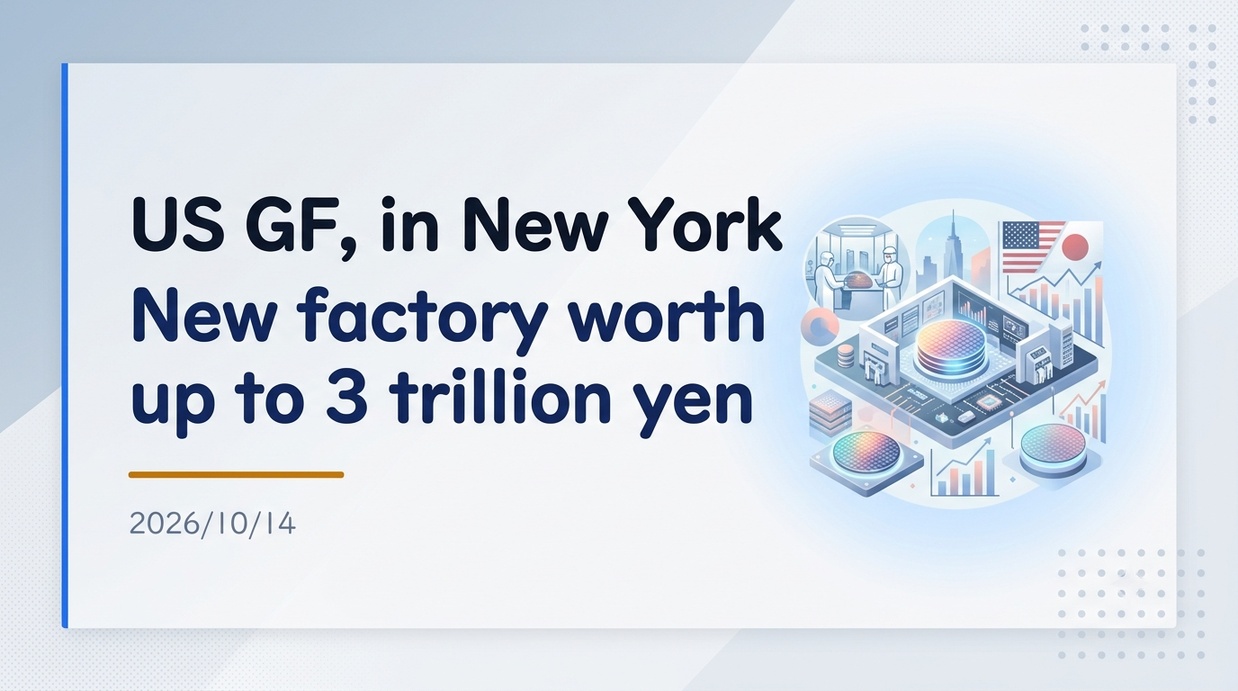
In October 2026, U.S. semiconductor foundry giant GlobalFoundries announced that, based on the Japan-U.S. strategic investment framework, it will construct and operate two new semiconductor plants worth up to $21 billion in New York State. This is a historic agreement in which the Japanese side will fund the entirety, dramatically strengthening the supply chain for mature and specialty semiconductors.
- Key Points of the Event and Investment Scheme
- Overview of New Factory Construction in Malta, New York
- Stock Market Reaction and Evaluation of US Semiconductor Foundry Manufacturing
- Job Creation and Opportunities for Japanese Companies and Related Supply Chains
- Strategic Intent in the Mature and Specialty Process Domain
- Future Outlook and Key Points
Key Points of the Event and Investment Scheme
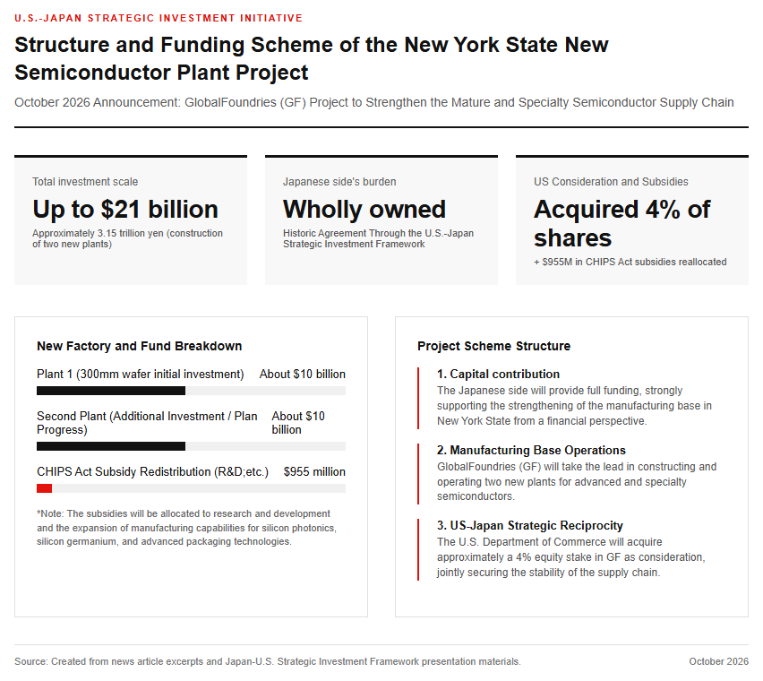
On October 14, 2026, major US foundry GlobalFoundries (GF) officially announced that it has been selected as the operator for two new semiconductor fabs at its manufacturing base in New York State, based on the US-Japan Strategic Investment Initiative. This initiative is promoted under a trade and investment agreement between US President Trump and the Japanese government, serving as a massive national project backed by a staggering investment of up to $21.0 billion (approximately 3.15 trillion yen). As for the specific investment scheme, an initial investment of approximately $10.0 billion will be made to begin construction of the first fab, which will support 300mm wafers. Furthermore, as the plan progresses, an additional $10.0 billion is scheduled to be allocated toward the construction of the second fab. Under this investment framework, the Japanese side will shoulder the entire funding amount, while the US Department of Commerce has agreed to acquire approximately a 4% equity stake in GF in return. In addition, GF has decided to amend its existing direct subsidy agreement under the US CHIPS Act, reallocating $955 million toward research and development and the expansion of manufacturing capabilities for silicon photonics, silicon germanium, and advanced packaging technologies. The following image represents a conceptual diagram of the next-generation manufacturing base resulting from the strategic partnership between the US and Japan.
Overview of New Factory Construction in Malta, New York
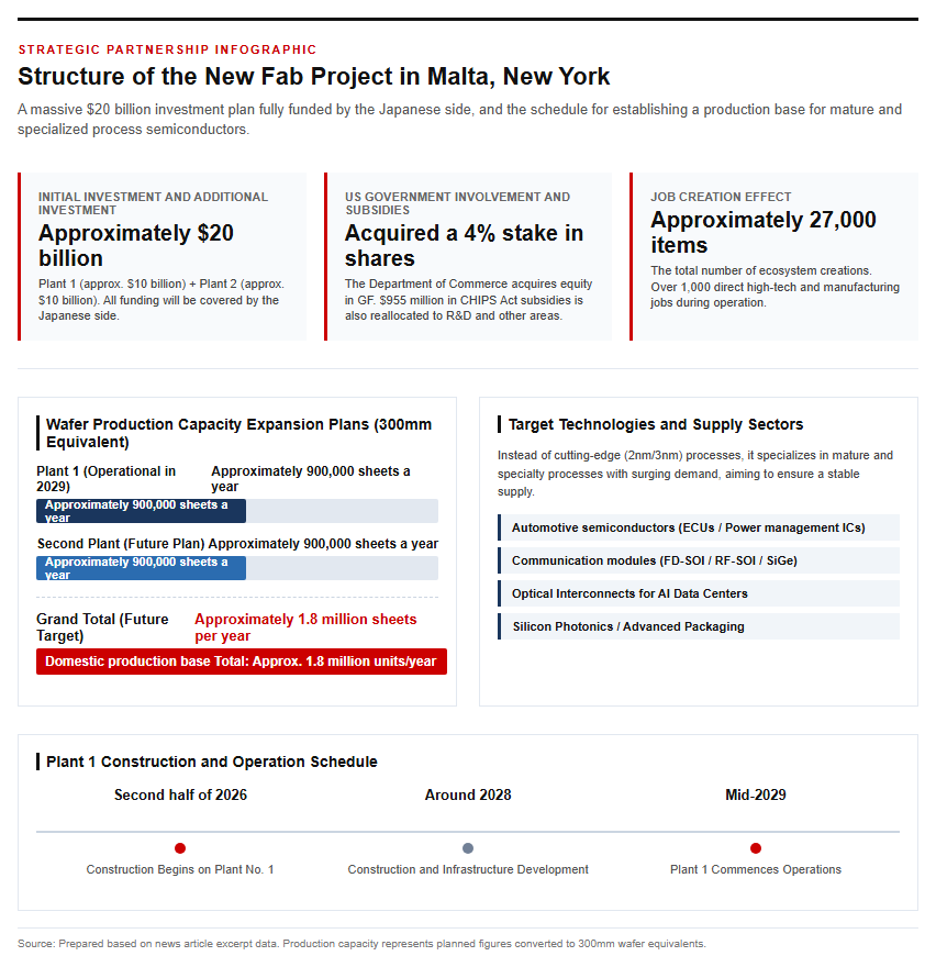
The new plant will be built on the expansive campus in Malta, New York, where GF is headquartered and operates its main facility (Fab 8). Construction of the first plant is scheduled to begin in the second half of 2026, with the aim of starting operations in 2029 following the construction work. Once the new plant reaches full capacity, the first plant alone is planned to add a manufacturing capacity of approximately 900,000 wafers per year (in 300mm wafer equivalents), and in the future, combined with a second plant, it is expected to create a massive domestic production base with a scale of approximately 1.8 million wafers per year. In 2018, GF froze its investment in the development of cutting-edge sub-10nm miniaturization processes, shifting its business strategy to specialize in mature and specialty process technologies such as FD-SOI, RF-SOI, and SiGe, in which it holds strengths for automotive and communications applications. Therefore, the new plant is not intended for cutting-edge 2nm or 3nm logic chips, but rather aims to provide a stable supply in the mature and specialty semiconductor fields—such as automotive electronic control units (ECUs), power management ICs, communication modules, and optical interconnects for AI data centers—where global demand is surging rapidly.
Impact on the Economy and Stock Markets, and Ripple Effects on the Supply Chain
Stock Market Reaction and Evaluation of US Semiconductor Foundry Manufacturing
Immediately after this historic agreement was announced, the stock price of GlobalFoundries (ticker: GFS), listed on the U.S. Nasdaq market, temporarily surged significantly by 4% to over 6%, eliciting a very strong and favorable response from the stock market. Wall Street investors and analysts highly praised the injection of massive capital into GF, the only “Trusted Foundry” (Category 1A) certified by the U.S. government, in addition to support for TSMC and Intel, which handle advanced nodes. Furthermore, expectations spread that the U.S. Department of Commerce holding a 4% equity stake would strengthen the public-private partnership and significantly alleviate GF’s mid- to long-term capital burden. On the other hand, some market participants voiced caution regarding the cyclical nature inherent to the semiconductor industry, the risk of declining fab utilization rates due to potential future stagnation in global demand, and the associated increase in fixed cost burdens, with future trends in the supply-demand balance being closely monitored.
Job Creation and Opportunities for Japanese Companies and Related Supply Chains
This project is expected to generate a tremendous job-creation impact on the economy of the Capital Region of New York State, where the manufacturing facility is located, as well as the entire United States. The broader ecosystem, including factory construction and surrounding infrastructure development, will create approximately 27,000 jobs, while factory operations are projected to directly generate over 1,000 advanced technical and manufacturing-related jobs. The conceptual images of the new factory’s construction site and the development of surrounding industries are shown below.
Furthermore, for the Japanese side contributing massive amounts of capital, this presents a prime opportunity for top-tier domestic semiconductor-related companies to deeply integrate into the supply chain. During the US-Japan negotiations, incentives are being sought such as the priority delivery of high-quality equipment and materials by manufacturing equipment makers like Tokyo Electron and semiconductor material manufacturers like Shin-Etsu Chemical and SUMCO, as well as the preferential supply of semiconductors to Japanese manufacturers based locally in the US. Major semiconductor manufacturer Renesas Electronics has already indicated a policy to utilize GF’s new plant capacity as an extension of its own production lines, and expectations are high for strengthened relationships with major customers, including Apple.
Semiconductor Geopolitics and Medium- to Long-Term Outlook
Strategic Intent in the Mature and Specialty Process Domain
Driven by escalating global US-China geopolitical risks and supply chain fragmentation, improving the domestic semiconductor self-sufficiency rate and strengthening economic security have become top priorities for both the US and Japanese governments. The United States is investing approximately $52 billion in subsidies under the CHIPS Act, and a trillion-yen-scale public funding race is unfolding worldwide, including the European Chips Act and Japan’s designation of specified critical materials. The shutdowns of automotive plants and production delays of electronic devices that became severe during the pandemic were directly caused by supply shortages of legacy and mature processes, rather than cutting-edge chips. The US government is strongly promoting the elimination of overseas dependency on mature semiconductors essential for defense equipment and critical infrastructure, and the role of GF, which has entered into a long-term supply contract of up to $3.1 billion over 10 years with the US Department of Defense (DoD), is critically important. This investment, utilizing the framework of the US-Japan alliance, will serve as a major milestone in completing the domestic supply chain for strategic materials across both military and industrial fronts.
Future Outlook and Key Points
The upcoming focus is the steady achievement of various milestones leading from the scheduled start of construction of the first plant in the second half of 2026 to the start of mass production in 2029. The smooth operation of fund management and profit-sharing mechanisms based on bilateral discussions between Japan and the U.S., as well as meeting technology development and facility completion standards based on the agreement with the U.S. Department of Commerce, will dictate future progress. Additionally, the speed of commercialization for cutting-edge technologies anticipating the AI era—such as silicon photonics, GaN (gallium nitride), and advanced packaging technologies utilizing the reallocated $955 million in funds—is also a major point of attention. How much Japanese manufacturing equipment and materials suppliers can enhance their global competitiveness through this project, and whether they can ride the wave of global semiconductor demand to maintain high operating rates, will hold the key to the project’s medium- to long-term success.
Reference page
- 【GlobalFoundries Annual Report on Form 20-F】https://www.sec.gov/ix?doc=/Archives/edgar/data/1709048/000170904825000024/gfs-20241231.htm
- 【GlobalFoundries Official Site】https://gf.com/
【#GlobalFoundries #Semiconductors #JapanUSInvestment #USEconomy #EconomicSecurity #SemiconductorPlant】
コメント