」を開設_en.png)
TOPPAN Inc. and the University of Tokyo’s Center for Advanced Science and Technology have established a donated research division aimed at the industrial application of quantum dot technology. Behind this lies the rapid expansion of the next-generation display and sensor markets, as well as the supreme task of strengthening competitiveness in domestic quantum technology.
- The five-year donated research division was launched.
- Fusion of Epitaxial and Colloidal Technologies
- Structural Transformation from Printing to Semiconductors and Advanced Materials
- Continuity from the Acquisition of the NS Materials Business
- Cadmium-free and compliance with environmental regulations
- Establishing valuation methods that meet market demands
- Growth Driven by Displays and Healthcare
- Ripple effects on solar cells and quantum computing
- Steps for Technology Implementation Toward 2031
- Producing Quantum-Native Talent
The five-year donated research division was launched.
TOPPAN Inc., a group company of TOPPAN Holdings, and the University of Tokyo Advanced Science and Technology Research Center (hereafter, UOF of Tokyo) have established the “Quantum Dot Innovation Lab (TOPPAN)” as a donated research division for five years, from July 1, 2026, to June 30, 2031. This project is operated as a basic fund funded by donations contributed by TOPPAN. The main goal is to combine the academic knowledge accumulated by the University of Tokyo Advanced Research Institute with TOPPAN’s cultivated nanoparticle synthesis technology and applied development capabilities.
As a specific research structure, Professor Yasuhiko Arakawa, an authority on epitaxial quantum dots, Professor Toru Tachima from the Colloidal Quantum Dots field, and Professor Yasuyuki Koseki from the University of Tokyo’s Institute of Advanced Studies will participate. Through close collaboration between industry and academia, a system has been established to tackle a wide range of themes, from controlling the physical properties of quantum dots to researching new quantum photonics devices and even pioneering optoelectronic fusion technologies.
Fusion of Epitaxial and Colloidal Technologies
A technical feature of this laboratory is its integrated research on two quantum dot technologies with different properties. One is epitaxial quantum dots, a technology that grows materials at the atomic layer level on semiconductor crystal substrates. With its high crystal quality and excellent optical properties, it is expected to be used as a single-photon emitting device essential for high-performance lasers and quantum information communication.
The other is the colloidal quantum dot, which was also awarded the 2023 Nobel Prize in Chemistry. These are nanoparticles produced through chemical reactions in liquids, allowing them to be coated and printed like ink, making them suitable for low-cost, large-area device manufacturing. TOPPAN has so far focused on applied development centered on colloidal quantum dots, but through this lab, by incorporating high-performance epitaxial quantum dot technology, we aim to lead device implementation technologies for realizing a sustainable society, such as next-generation displays, energy generation, and optoelectronic fusion. Please refer to the diagram below.
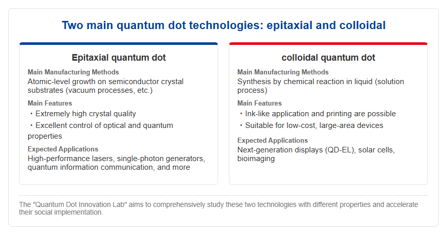
Management and Strategy Background: Why TOPPAN Focuses on Quantum Dots
Structural Transformation from Printing to Semiconductors and Advanced Materials
TOPPAN is currently driving a dramatic structural transformation from its traditional printing business to a high value-added business centered on semiconductors and advanced materials. In April 2026, we integrated the three major companies within the group and transitioned to a new operational structure centered on DX (Digital Transformation) and SX (Sustainable Transformation). Within this strategy, quantum dots are positioned as the next growth engine for the electronics business.
In fact, the company is accelerating its investment in advanced semiconductors, such as doubling its production capacity for FC-BGA substrates for AI and data centers compared to fiscal year 2022. The establishment of quantum dot technology not only creates synergies with these semiconductor-related businesses but also serves as a crucial stepping stone for the company, which holds world-class photomask technology, to dominate the next-generation device market with an eye toward 2030.
Continuity from the Acquisition of the NS Materials Business
The commitment to quantum dots is an extension of strategic moves made over the past several years. On August 1, 2023, TOPPAN acquired the relevant business from NS Materials Co., Ltd., which was engaged in the development of quantum dots and nanomaterials. Through this, TOPPAN has strengthened its vertically integrated development system, handling everything from quantum dot synthesis to device implementation.
The opening of the lab with the University of Tokyo Advanced Research Institute is also a “supplement of knowledge” to further accelerate in-house commercialization. By building an environment where advanced external academic knowledge can be continuously incorporated, we aim to transform beyond being a mere material supplier to become a total solution provider for next-generation optical and electronic devices. Regarding research and development expenses, we are continuously expanding investment in advanced technologies, with expectations of 31 billion yen in the fiscal year ending March 2025.
Market and Technology Challenges: Environmental Regulations and Stability to Overcome
Cadmium-free and compliance with environmental regulations
One of the biggest barriers to the social implementation of quantum dot technology is compliance with environmental regulations. Early quantum dots often contained harmful heavy metals such as cadmium selenide, and their use in electronic devices was strictly restricted by European RoHS directives and other regulations.
At this laboratory, developing high-quality materials that comply with these environmental regulations is one of our top priorities. Currently, the market is shifting toward cadmium-free materials such as indium phosphide (InP), but precise surface control technology at the nanoscale is essential to consistently deliver optical performance comparable to Cd systems. By collaboratively solving technical challenges such as defect suppression at interfaces and ensuring stability in the atmosphere, we aim to create competitive products that meet global standards.
Establishing valuation methods that meet market demands
Quantum dots are expected to be utilized in a wide range of fields, such as next-generation displays and high-sensitivity sensors, but precise evaluation methods to ensure their quality are still developing. Accurately capturing the unique behavior of nanomaterials and the changes over time when integrated into devices is a major hurdle to mass production.
In this lab, we will also research methods to visualize and evaluate the physical property control of quantum dots at the nanoscale by utilizing Professor Yasuyuki Koseki’s quantum photometric measurement techniques. Through this, we plan not only to improve material quality but also to promote foundational technologies in synthesis and coating processes, thereby raising the overall level of Japan’s domestic quantum dot industry. Please refer to the diagram below.
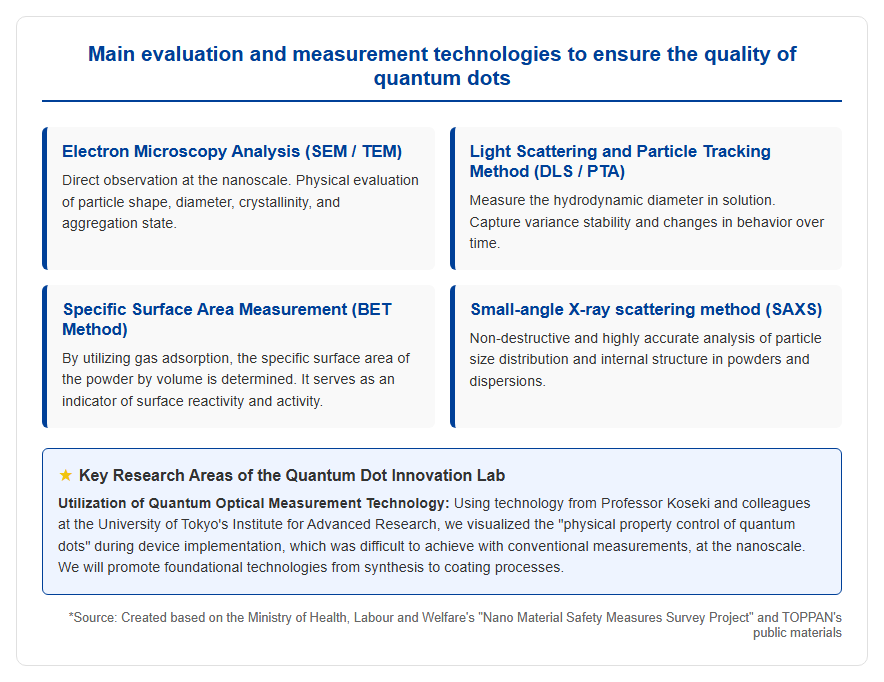
Market potential: The Japanese market to exceed $2.2 billion by 2034
Growth Driven by Displays and Healthcare
Japan’s quantum dot market is expected to experience remarkable growth over the next decade. According to research reports, the domestic market size, which was approximately USD 674.5 million in 2025, is expected to reach USD 2.2708 billion by 2034, with a compound annual growth rate (CAGR) of 14.44%. A major driver of this growth is the demand for next-generation displays that balance color reproduction with energy efficiency.
The expansion of adoption in the healthcare sector is also noteworthy. Quantum dots are gaining value as fluorescent probes that provide higher brightness and greater photostability than conventional organic dyes in bioimaging, drug delivery (drug delivery), and disease diagnosis. The research results at this lab are expected to serve as a driving force to strengthen Japan’s presence in these high-growth markets.
Ripple effects on solar cells and quantum computing
The application scope of quantum dots extends beyond displays to include renewable energy and advanced computing fields. In particular, quantum dot solar cells have the potential to dramatically improve theoretical energy conversion efficiency by adjusting the band gap to capture a wide spectrum of light, including infrared.
Furthermore, in the field of quantum computing, research is progressing as a quantum bit material combined with silicon chips. The collaboration between TOPPAN and the University of Tokyo Advanced Research Institute is expected to serve as a hub for securing Japan’s technological initiatives in these emerging fields. By advancing basic research with a view to diverse applications, we aim to secure a competitive edge in the global market, which is expected to reach a future value of 33.8 billion USD.
Future Developments and Focus: Roadmap for Social Implementation and Human Resource Development
Steps for Technology Implementation Toward 2031
The Quantum Dot Innovation Lab aims to deepen a systematic understanding of science and technology related to quantum dots over five years until 2031, establishing a foundation that will contribute to future industrial applications. In the initial phase, we will focus on controlling material properties and establishing high-quality synthesis processes, and in the mid-term and later, we plan to advance not only to next-generation displays but also to prototypes of ultra-high-speed communication devices using optoelectronic fusion technology and highly efficient energy conversion devices.
Of particular note is the progress toward the practical application of self-emissive quantum dot displays (QD-EL), which had previously been considered difficult. If we can take a step beyond traditional hybrid methods and realize the ultimate device structure where quantum dots emit light directly, it will undoubtedly become a game changer in the display industry.
Producing Quantum-Native Talent
Another important role of this lab is to cultivate talent who will lead the next generation of quantum technologies. TOPPAN aims to foster “Quantum Natives” and runs an in-house educational program that enables students to acquire master’s-level knowledge over three years. By increasing opportunities to experience advanced university research environments through this lab, we will accelerate this trend.
An environment where motivated researchers can interact across industry-academia boundaries and simultaneously learn the latest theories and real-world industrial challenges forms the foundation of Japan’s quantum technology ecosystem. Rather than just developing technology, producing about 100 people who can master and implement those technologies in society will be the true results that will be tested by the end of the project five years from now.
[#TOPPAN #東大先端研 #量子ドット #量子技術 #半導体 #産学連携 #次世代ディスプレイ #ナノテクノロジー]

コメント