Samsung Electronics has begun placing orders for additional equipment aimed at mass-producing 2nm semiconductors at its Taylor plant in Texas, USA. This move is driven by the growing demand for advanced semiconductor contract manufacturing within the United States and intensifying competition to secure orders from major IT companies.
- Equipment Move-in and Plans for the Final Stage of 2nm Mass Production
- Yield Improvement and Technological Advancements in Manufacturing Processes
- Securing orders and supply contracts from Tesla and major IT companies
- TSMC’s “N-2 Rule Constraints” and the Inflow of Third-Party Demand
- Finalization of US CHIPS Act Subsidies and Political Concerns
- Construction Plan for the Second Plant and Future Focus Points in the Foundry Market
Equipment Move-in and Plans for the Final Stage of 2nm Mass Production
In October 2026, Samsung Electronics began the final stage of capital investment for the mass production of 2nm semiconductor processes at its first fab under construction in Taylor, Texas, USA. In the initial stage, manufacturing equipment capable of a monthly production capacity of approximately 6,000 wafers will be sequentially installed, with the goal of expanding production to 20,000 wafers per month by mid-2027. Construction of the Taylor plant began in 2022, and Samsung has made a massive cumulative investment of approximately $37 billion throughout central Texas. The following figure illustrates the overall concept of the Taylor plant.
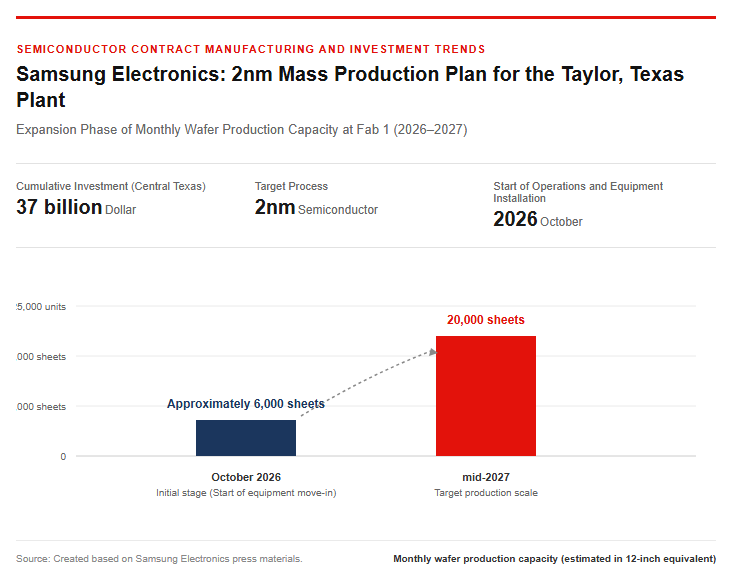
The factory is scheduled to begin operations by the end of 2026, with plans to transition to full-scale mass production of 2nm chips using extreme ultraviolet (EUV) lithography technology starting in 2027. This equipment order represents a crucial step for the company in establishing an advanced process contract manufacturing system locally in the United States.
Yield Improvement and Technological Advancements in Manufacturing Processes
The yield rate (yield), which was the biggest challenge in the mass production of the 2nm process, is improving rapidly. The yield for “SF2,” the first-generation 2nm process, rose from the 30% range as of mid-2025 to the 50% range in January 2026, to approximately 55% in August of the same year, and to about 60% in late September, eventually reaching approximately 80% as of October 2026, achieving mass-production levels. The SF2 process adopts the GAA (Gate-All-Around) structure, which precisely controls current flow. Furthermore, Samsung is concurrently proceeding with the deployment of “SF2P,” a second-generation 2nm process. The SF2P process is expected to deliver a 12% improvement in performance, a 25% reduction in power consumption, and an 8% decrease in chip area compared to conventional processes. The stabilization of yields and reduction of manufacturing costs serve as a critically important foundation for acquiring new customers in the foundry market.
Major Customer Acquisition Trends and Demand in the U.S. Market
Securing orders and supply contracts from Tesla and major IT companies
Taylor Fab 1 has secured sufficient orders for its 2nm manufacturing capacity even before the start of mass production. In July 2025, Samsung signed a long-term semiconductor foundry contract with Tesla valued at approximately $16.5 billion (approx. 22.7648 trillion won), valid until the end of 2033. Under this contract, production of Tesla’s next-generation “AI6” and “AI5” chips is scheduled to take place at the Taylor plant. Furthermore, major companies such as communication semiconductor provider Broadcom, smart device IP provider Arm, and edge AI platform provider Ambarella have also decided to utilize the 2nm process. The following figure illustrates the supply chain collaboration with customers.
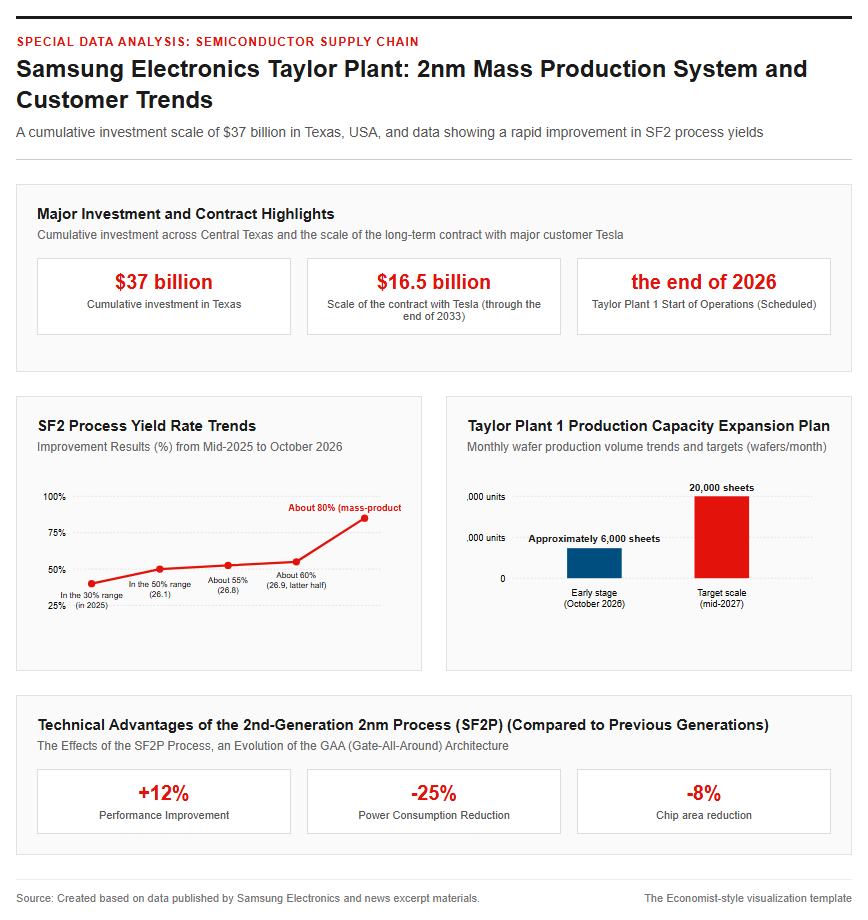
In addition, Google, which is promoting the external sales of its in-house developed TPUs, and major processor manufacturer AMD are also in discussions regarding prototyping and production allocation at the same fab, steadily expanding the order-receiving base within the United States.
TSMC’s “N-2 Rule Constraints” and the Inflow of Third-Party Demand
TSMC, the world’s largest foundry, boasts a 72.5% market share as of the second quarter of 2026, maintaining a massive gap over Samsung’s 5.9%. However, the majority of TSMC’s 2nm production capacity is already booked by major clients such as Apple and Nvidia, leaving little room in its supply capacity. Furthermore, due to the Taiwan government’s “N-2 rule” (a regulation permitting overseas production only for technology two generations behind the most advanced node), chips produced at TSMC’s Arizona fab in 2027 are expected to remain at the 3nm process. As a result, for Big Tech companies like AMD, Qualcomm, and Google that wish to procure cutting-edge 2nm chips within the United States, Samsung—with its 2nm fab in the U.S.—is emerging as a major alternative choice.
Policy Support, Geopolitical Risks, and Future Outlook
Finalization of US CHIPS Act Subsidies and Political Concerns
Samsung’s massive investment in Texas is backed by policy support from the U.S. government. In December 2024, the U.S. Department of Commerce finalized and announced a direct subsidy of up to $4.745 billion (approximately 700 billion yen) to Samsung under the CHIPS and Science Act. This funding will support two advanced logic semiconductor manufacturing facilities and an R&D facility in Taylor, as well as the expansion of the Austin plant. Meanwhile, under the Trump administration, policy uncertainty associated with political shifts has emerged, with discussions about requiring the acquisition of equity stakes in recipient companies as a condition for subsidy disbursement and the potential review of existing contracts being raised. The South Korean semiconductor industry is carefully monitoring the potential impact of receiving the subsidies on shareholder value and the trends in regulatory changes.
Construction Plan for the Second Plant and Future Focus Points in the Foundry Market
Samsung plans to begin construction on its second Taylor plant in early November 2026, anticipating a further expansion of its supply capacity. The second plant will be approximately 1.5 times the size of the first, with a goal of mass-producing 2nm chips by 2030. By running its Pyeongtaek fab in South Korea and the Taylor plant in the U.S. in parallel, the company aims to achieve profitability in its non-memory business division starting in the fourth quarter of 2026. Key points to watch in the foundry market going forward include stabilizing equipment operations at the first Taylor plant, demonstrating power-efficiency performance in mass-produced products, and presenting a stable supply schedule to customers. Whether these massive upfront investments can be translated into a recovery in contract manufacturing market share will be a major turning point in determining future semiconductor supremacy.
Reference Page
- [U.S. Department of Commerce Press Release] https://www.commerce.gov/news/press-releases/2024/12/biden-harris-administration-announces-chips-incentives-award-samsung
【#Semiconductor #Samsung #2nm #Foundry #CHIPSAct #AIChip #TSMC】

コメント