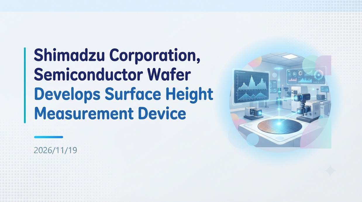
Shimadzu Corporation has jointly developed a surface height measurement device for semiconductor wafers with AI Mechtech. This development is driven by the rapid spread of generative AI, which has led to expanding demand for advanced packaging technology, as well as strong market requirements for improving yields and early defect detection in back-end processes.
- Overview and Development Objectives of the Wafer Surface Height Measurement System
- Advances in Advanced Packaging Technology and Sophisticated Quality Control Requirements
- Business Development Centered on Turbomolecular Pumps and Surface Analysis Technology
- Growth Trends in the Global Semiconductor Inspection and Metrology Equipment Market
- Contribution to Synergy and Productivity Enhancement through Joint Development
- Future Outlook and Contribution to a Sustainable Semiconductor Industry
Overview and Development Objectives of the Wafer Surface Height Measurement System
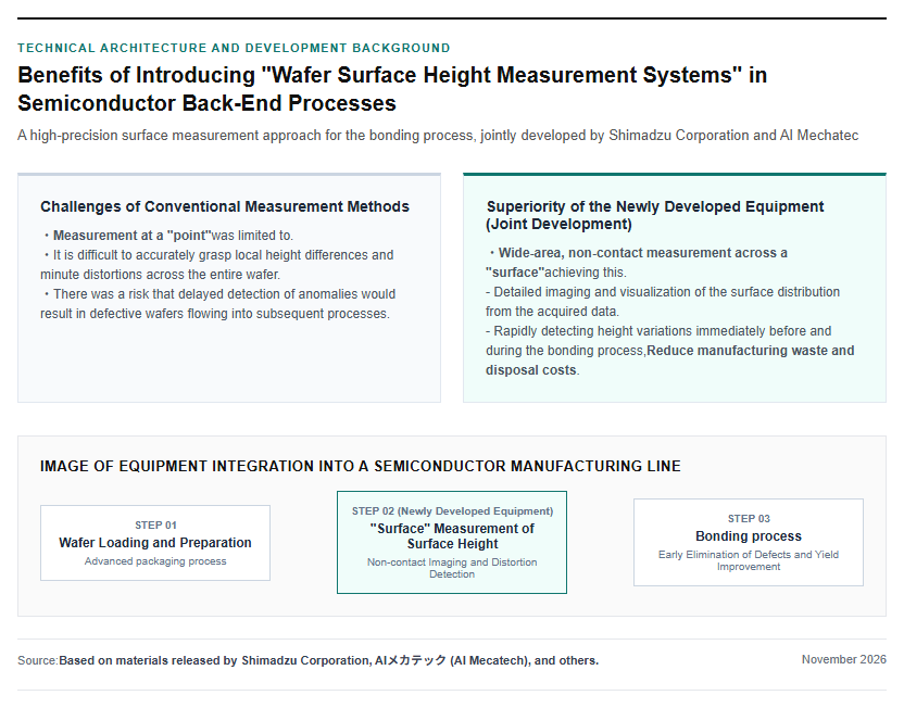
On November 18, 2026, Shimadzu Corporation, a major analytical and measuring instruments manufacturer, announced that it has jointly developed a wafer surface height measurement system with semiconductor manufacturing equipment maker AI Mechatec. This system is used by being integrated into bonding equipment that joins wafers together with high precision in semiconductor manufacturing. Because conventional measurement methods could only measure height at discrete points, it was difficult to accurately grasp local height differences and distortions across the entire wafer. In contrast, this system has the advantage of performing non-contact, wide-area measurements of the entire wafer surface as a plane, enabling detailed imaging and visualization of the surface distribution from the acquired height data. It was realized by bringing together Shimadzu’s accumulated precision control, optical measurement, and image processing technologies. By quickly detecting height irregularities immediately before or during the bonding process, it can prevent defective wafers with anomalies from being fed into subsequent processes. It strongly supports the early detection of defects in back-end semiconductor manufacturing processes and will greatly contribute to reducing manufacturing losses and disposal costs. The following figure shows an image of the device integrated into a semiconductor manufacturing line.
Advances in Advanced Packaging Technology and Sophisticated Quality Control Requirements
In recent years, against the backdrop of the rapid penetration of generative AI, high-performance computing (HPC), and the evolution of automotive electronics, demand for advanced packaging technology that stacks and connects multiple semiconductor chips at high densities has been increasing remarkably. To improve semiconductor performance, in addition to conventional circuit miniaturization (front-end processes), increasing density in packaging (back-end processes)—as represented by 3D stacking, chiplet structures, and high-bandwidth memory (HBM)—has become extremely crucial. In these manufacturing processes, the bonding step of precisely bonding wafers together is a core process that dictates chip electrical conductivity and heat dissipation performance. This equipment features an exceptionally superior height resolution of 0.1 μm or less. 0.1 μm is 0.0001 mm, an extremely minute dimension equivalent to approximately one-thousandth the thickness of a human hair. By visualizing wafer surface distortion and local thickness variations in real time at this micro-scale, it becomes possible to eliminate defects associated with void generation and misalignment during bonding. It is highly anticipated as an in-line measurement tool that simultaneously achieves improved yields and enhanced productivity on manufacturing lines. The following figure is a conceptual diagram of the wafer bonding process in advanced packaging.
Shimadzu Corporation’s Semiconductor Business Strategy and Market Environment
Business Development Centered on Turbomolecular Pumps and Surface Analysis Technology
Shimadzu Corporation is accelerating the expansion of its semiconductor market solutions in both analytical measuring instruments and vacuum/industrial equipment. In the company’s industrial equipment segment, sales of turbomolecular pumps (TMPs), which are essential for creating the vacuum environments required in semiconductor manufacturing, have been performing extremely well in Japan, Europe, Taiwan, South Korea, and other regions. In its financial results for the first quarter of the fiscal year ending March 31, 2027 (April–June 2026), the industrial equipment segment’s net sales increased 23% year-on-year to 20.7 billion yen, and operating profit before the amortization of goodwill and other items rose 44% year-on-year to 3.8 billion yen, strongly driving record-high consolidated net sales of 130.596 billion yen (a 10% increase year-on-year). Furthermore, in July 2026, the company made Tescan Group, a major Czech electron microscope manufacturer, a wholly owned subsidiary. By acquiring Tescan’s technology, which excels in scanning electron microscopes (SEMs) and focused ion beam systems (FIB-SEMs), Shimadzu has integrated the three major elements of research and analysis: surface observation, physical property measurement, and compositional analysis. As a result, the company has established a framework for providing integrated analysis solutions that cover the entire semiconductor manufacturing process, ranging from front-end defect analysis to back-end in-line inspection.
Growth Trends in the Global Semiconductor Inspection and Metrology Equipment Market
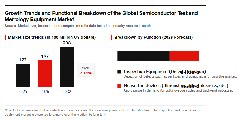
The global semiconductor inspection and metrology equipment market continues to expand rapidly, driven by the advancement of manufacturing processes and the increasing complexity of chip structures. According to an industry research report, the market size is projected to grow from 17.2 billion USD in 2025 to 19.7 billion USD in 2026, and reach 29.8 billion USD by 2032. The compound annual growth rate (CAGR) from 2026 to 2032 is estimated at approximately 7.14%. Looking at the market composition by function, inspection equipment, which detects defects such as particles and scratches, accounts for 64.00%, while metrology equipment, which measures dimensions, flatness, and film thickness with high precision, accounts for 36.00%. While inspection equipment drives the overall market scale, metrology equipment plays an indispensable role as the cornerstone of process control in advanced nodes and three-dimensional structures. Traditionally, demand for metrology equipment has centered on front-end processes such as lithography and thin-film deposition, but with the proliferation of advanced packaging and HBM, demand for high-precision metrology in back-end processes is surging rapidly. Supported by wafer fab expansions and line automation investments in key regions such as China, South Korea, Taiwan, and North America, the market is expected to see continued medium- to long-term expansion.
Future Outlook and Societal Impact on Semiconductor Manufacturing
Contribution to Synergy and Productivity Enhancement through Joint Development
This product development is the result of fusing Shimadzu Corporation’s advanced control, optical, and image processing technologies with the mechanism and automation technologies for semiconductor bonding equipment that AI Mechtech has cultivated over many years. By integrating this measurement unit directly into the bonding equipment offered by AI Mechtech, semiconductor manufacturers and OSATs (outsourced semiconductor assembly and test providers) will be able to automatically measure the height of the entire wafer without stopping the line. Feeding measurement data back to the equipment in real time enables the optimization of processing conditions such as temperature and pressure during bonding, as well as the preliminary detection of equipment abnormalities. Furthermore, the automation of quality judgments that previously relied on the expertise of skilled operators will advance, offering the significant benefit of eliminating the reliance on specific individuals in the lab. By promoting the automation and smartification (smart factory implementation) of the entire manufacturing process, the defect rate will be drastically reduced, enabling a substantial improvement in manufacturing throughput and stable mass production. The following figure shows the workflow of smart manufacturing using quality monitoring data.
Future Outlook and Contribution to a Sustainable Semiconductor Industry
In its mid-term vision “Shimadzu 2035,” Shimadzu Corporation aims to achieve net sales of 1 trillion yen by 2035, positioning the semiconductor field as its top priority area for growth. Based on its core vacuum and measurement technologies, the company is deploying the “Analytical Intelligence” concept—which integrates AI technology and software—advancing its evolution from a mere equipment vendor into a problem-solving total solution provider. Improving yields and enabling the early detection of defects in semiconductor manufacturing go beyond mere cost reduction; they directly lead to reductions in the consumption of electricity, silicon wafer resources, and various chemical reagents used throughout the manufacturing process. As reducing environmental impact and ensuring sustainability become top global priorities for the semiconductor industry, Shimadzu’s initiatives to contribute to maximizing resource efficiency and reducing waste through high-quality measurement technology are expected to deliver even greater value within the global semiconductor supply chain moving forward.
Reference page
- [Shimadzu Corporation News Release] https://www.shimadzu.co.jp/news/2026/vp7lm1_ptac01s6n.html
- [AI Mechtech, Inc. News Release] https://www.ai-mech.com/wp-content/uploads/2026/11/cb01c9a494b5cbff976ea226f26eb9ce.pdf
[#Shimadzu #AIMechatech #Semiconductors #AdvancedPackaging #WaferMeasurement #YieldImprovement #ScienceAndTechnology]


コメント