As part of its growth strategy, the Ministry of Economy, Trade and Industry (METI) has formally designated the region centered around Higashihiroshima, Kure, and Fukuyama cities in Hiroshima Prefecture as a national specified semiconductor cluster hub. Behind this decision are a massive capital investment of approximately 1.5 trillion yen by U.S.-based Micron Technology and a national policy objective of establishing a regional industrial base that is resilient to geopolitical risks.
- Background and Key Points of Higashihiroshima, Kure, and Fukuyama Being Selected as National Hubs
- Breaking Away from Automobile Dependence and Transitioning to a Two-Legged Industrial Structure
- 1.5 Trillion Yen Investment in the Higashi-Hiroshima Facility and Production Expansion Plans for Advanced DRAM and HBM
- Capital Investment and Technological Collaboration of Related Companies in Surrounding Areas, Including Kure and Fukuyama
- Geographical Advantages and Prerequisites for Cybersecurity Measures and Infrastructure Development
- Talent Development Initiatives and Key Focus Areas Toward 2030
Background and Key Points of Higashihiroshima, Kure, and Fukuyama Being Selected as National Hubs
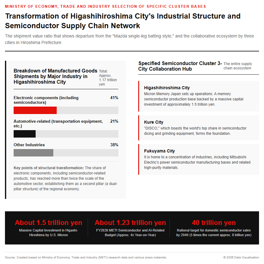
In May 2026, toward the formulation of a public-private investment roadmap, the government’s Growth Strategy Headquarters selected eight regions out of the designated target areas nationwide as specified semiconductor clusters. Among them, the area comprising Higashihiroshima, Kure, and Fukuyama cities in Hiroshima Prefecture was positioned as a core accumulation hub in the Chugoku region. The Ministry of Economy, Trade and Industry’s semiconductor and AI-related budget for fiscal 2026 has been significantly expanded to approximately 1.23 trillion yen, about four times that of the previous year, making it a key area for achieving the national goal of increasing domestic semiconductor sales to 40 trillion yen annually by 2040 (a fivefold increase from the current approximately 8 trillion yen). Higashihiroshima City is home to major memory semiconductor maker Micron Memory Japan, Kure City hosts DISCO, which boasts the world’s top market share in semiconductor dicing and grinding equipment, and Fukuyama City concentrates Mitsubishi Electric’s power semiconductor manufacturing bases and related industries. By having these three adjacent cities work together in an integrated manner, a robust ecosystem is formed across the entire semiconductor supply chain, ranging from front-end to back-end processes, as well as manufacturing equipment and high-purity materials.
Breaking Away from Automobile Dependence and Transitioning to a Two-Legged Industrial Structure
For many years, Hiroshima Prefecture’s economy has relied on the transportation machinery industry, centered around the global automaker Mazda. In Higashihiroshima City as well, an industrial structure described as the “Mazda single-leg batting style” had persisted for a long time, but recent economic data confirms that a structural transformation is underway at a dramatic pace. According to a survey by the Ministry of Economy, Trade and Industry, out of Higashihiroshima City’s manufactured goods shipments of approximately 1.17 trillion yen, the proportion of electronic components including semiconductors has reached 41%, already significantly surpassing the 21% share of automotive-related industries by more than double. As Mazda faces earnings fluctuations amidst global tariff risks and the transition to electrification, the establishment of semiconductors as a second pillar directly linked to global demand serves as a powerful cushion to offset the vulnerability of the regional economy as a whole. The direct economic effects brought by massive semiconductor investments—such as job creation from the construction and expansion of factories, rising housing demand, and increased activity among construction workers—are already strongly supporting the regional economy. The following chart shows the transition in the shipment value proportions of major industries in Higashihiroshima City and the diversification of its industrial structure into a two-pillar model.
Micron’s 1.5 Trillion-Yen Investment and the Concentration of Local Supply Chains
1.5 Trillion Yen Investment in the Higashi-Hiroshima Facility and Production Expansion Plans for Advanced DRAM and HBM
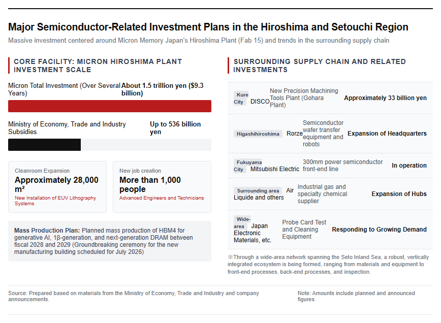
At the core of the selection of this specific cluster is a large-scale investment project at the Hiroshima Plant (Fab15) of Micron Memory Japan, a subsidiary of U.S.-based Micron Technology. A groundbreaking ceremony for the new manufacturing building was held on July 4, 2026, with a total investment of approximately 1.5 trillion yen (approx. $9.3 billion) to be made over the next few years. The Ministry of Economy, Trade and Industry has decided to provide a subsidy of up to 536 billion yen through the specified semiconductor fund and other means. In this expansion project, a new cleanroom of approximately 28,000 square meters will be constructed, and mass production of High Bandwidth Memory (HBM4)—for which demand is rapidly growing for generative AI—as well as 1-beta generation and next-generation DRAM is scheduled from fiscal 2028 to 2029. Extreme ultraviolet (EUV) lithography equipment is scheduled to be newly introduced into the new manufacturing building, which will bring the world’s most advanced miniaturization process into full-scale operation in Japan. This mega-project is expected to create new jobs for more than 1,000 advanced technicians and engineers, greatly contributing to the creation and retention of high-wage employment in the local economy.
Capital Investment and Technological Collaboration of Related Companies in Surrounding Areas, Including Kure and Fukuyama
In tandem with Micron’s massive investment, surrounding manufacturing equipment and materials makers in cities such as Kure and Fukuyama are also accelerating large-scale capital investments. In Kure, major dicing equipment manufacturer DISCO will begin construction in February 2026 on a new plant dedicated to precision processing tools at its Gohara Plant, investing approximately 33 billion yen, with operations targeted to start in April 2028. Rorze, a major semiconductor transport equipment manufacturer headquartered in Higashihiroshima, supplies wafer transfer robots to fabs worldwide and continues to expand its headquarters functions in line with business growth. In Fukuyama, in addition to Mitsubishi Electric’s power semiconductor front-end line compatible with 300mm wafers, industrial gas makers such as France’s Air Liquide and suppliers handling specialty chemicals are proceeding with expanding their bases. Furthermore, mid-sized and small enterprises such as Japan Electronic Materials, which handles inspection probe cards; Teraprobe, which provides contract testing; and J.E.T., which produces cleaning equipment, are also riding the wave of demand, rapidly expanding a wide-area semiconductor supply chain across the Seto Inland Sea, as shown in the figure below.
Economic Security and Regional Challenges: Future Prospects
Geographical Advantages and Prerequisites for Cybersecurity Measures and Infrastructure Development
One of the key reasons why Hiroshima Prefecture was selected as a national semiconductor cluster is its geographical advantage of extremely low natural disaster risk. Compared to the Tokyo metropolitan area and other coastal regions, Hiroshima Prefecture has an extremely low probability of “less than 3%” of a major earthquake with a seismic intensity of lower 6 or higher occurring within the next 30 years. For advanced semiconductor factories that require precise positional control and continuous operation, this low seismic risk is a decisive strength. Meanwhile, there are also strict challenges regarding the strengthening of the production base. The Ministry of Economy, Trade and Industry has outlined a policy to make the establishment of robust defense systems against cyberattacks and the mitigation of supply disruption risks as grant conditions for semiconductor factory subsidies from fiscal 2026 onward. Strong demands are being placed on protecting visual information on manufacturing lines, restricting room entry, segmenting networks, and establishing early recovery systems. Furthermore, how swiftly to proceed with easing traffic congestion around Higashihiroshima City, securing a stable supply of industrial water and electricity, and relaxing land-use regulations such as the conversion of agricultural land and the release of protection forests will be the key to eliminating growth bottlenecks.
Talent Development Initiatives and Key Focus Areas Toward 2030
The most critical challenge for the Hiroshima cluster to continue growing over the medium to long term is securing advanced semiconductor-related talent and specialized engineers. Partnering with local major universities and technical colleges, including Hiroshima University, Micron has offered over 80 outreach classes and lectures over a four-year period, implementing a development program with a cumulative total of more than 2,900 participating students. Furthermore, Hiroshima Prefecture is strongly urging the national government for financial support to provide hands-on manufacturing experiences starting from the primary and secondary education levels, increase university enrollment capacities, and improve the settlement environment for highly skilled foreign human resources. In the Japanese government’s national strategy targeting 15 trillion yen in semiconductor sales by 2030 and 40 trillion yen by 2040, the Hiroshima cluster in the Chugoku region is positioned as a key hub for industrial restructuring, alongside Rapidus in Hokkaido and TSMC Kumamoto in Kyushu. Moving forward, the global semiconductor market will closely monitor the progress of manufacturing equipment installation into Micron’s new building, which began construction in May 2026, the further accumulation of materials and inspection equipment manufacturers related to EUV lithography, and the results leading up to full-scale shipments slated for 2028–2029.
Reference Page
- [Ministry of Economy, Trade and Industry] https://www.meti.go.jp/
- [Ministry of Economy, Trade and Industry: Certified Plans for the Establishment of Specified Semiconductor Production Facilities] https://www.meti.go.jp/policy/mono_info_service/joho/laws/semiconductor/semiconductor_plan.html
- [Micron Memory Japan] https://jp.micron.com/
【#SemiconductorCluster #MinistryOfEconomyTradeAndIndustry #Micron #Higashihiroshima #EconomicSecurity #AISemiconductors】

コメント