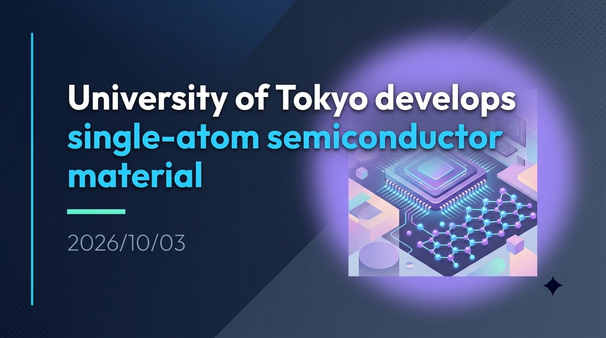
An international research group including the University of Tokyo has developed “BCN,” a next-generation p-type two-dimensional semiconductor material that is only one atom thick, and successfully achieved wafer-scale film formation. This development is driven by the physical limits of miniaturization in conventional silicon semiconductors and the intensifying global race to develop advanced semiconductors with an eye on the post-silicon era.
- The Full Picture of BCN: A New Material with the Thickness of a Single Atom Developed by the University of Tokyo
- The Technical Advantages of 2D Semiconductors That Break Conventional Silicon Limits
- Strong partnership with Taiwan’s TSMC and roadmap for mass production by 2031
- The Battle for Supremacy at 2nm and Beyond in the Advanced Semiconductor Foundry War
- Ripple Effects on Japanese Semiconductor Material and Equipment Manufacturers and Promising Stocks
- Challenges and Prospects for the Practical Application of Next-Generation Complementary Metal-Oxide-Semiconductor (CMOS) Circuits
The Full Picture of BCN: A New Material with the Thickness of a Single Atom Developed by the University of Tokyo
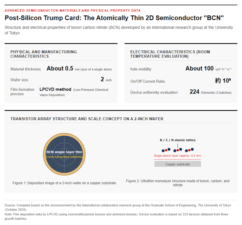
In October 2026, an international joint research group including Professor Vincent Tan and Assistant Professor Lehan Hu at the Graduate School of Engineering, The University of Tokyo, announced that they have successfully developed “boron carbonitride (BCN)” which operates as a next-generation p-type two-dimensional semiconductor by densely incorporating carbon atoms into the crystal lattice of a single atomic layer of boron nitride (BN). The newly developed material features an ultra-thin, single-atom structure with a thickness of only about 0.5 nanometers. Using low-pressure chemical vapor deposition (LPCVD), the research team precisely controlled the decomposition and reaction pathways of two source molecules: monomethylamine borane and ammonia borane. This established a process that suppresses the rapid aggregation of carbon on a copper substrate and grows a uniform monolayer film across a 2-inch wafer. The fabricated BCN transistors exhibited exceptional electrical properties, including a hole mobility of approximately 100 cm² V⁻¹ s⁻¹ and an on/off current ratio of about 10⁸ at room temperature. Furthermore, high uniformity in characteristics was confirmed in the evaluation of 224 devices fabricated across three growth batches. The figure below shows the structure of the transistor array fabricated on a 2-inch wafer.
This achievement is a groundbreaking breakthrough that has demonstrated, for the first time in the world, the simultaneous realization of large-area scalability and high mobility in p-type two-dimensional materials, which had previously been considered difficult.
The Technical Advantages of 2D Semiconductors That Break Conventional Silicon Limits
Silicon semiconductors, currently used as the brains of all digital devices, are facing severe physical barriers as circuit line widths are miniaturized into the sub-1-nanometer region: the short-channel effect, where current control by the gate electrode becomes ineffective, and a significant increase in leakage current. Gaining worldwide attention as a promising solution to break through this limitation are “two-dimensional semiconductors,” which have a thickness of only one to a few atomic layers. Two-dimensional semiconductors exhibit high charge mobility while maintaining an ultrathin channel layer, offering the advantage of strongly suppressing the short-channel effect even when miniaturized. To construct complementary metal-oxide-semiconductor (CMOS) circuits, which form the basic framework of modern electronic circuits, both n-type (carrying electrons) and p-type (carrying holes) are indispensable. However, in conventional two-dimensional material research, while high performance has been achieved in n-type semiconductors represented by molybdenum disulfide (MoS₂), the creation of comparable high-quality p-type materials and growth technology on large-area wafers have been global bottlenecks. With the advent of this new BCN material, both n-type and p-type semiconductors are now available on a wafer scale, completing the foundation for the realization of next-generation three-dimensional integrated circuits and ultra-low-power chips.
TSMC Partnership and Impact on the Global Industrial Structure
Strong partnership with Taiwan’s TSMC and roadmap for mass production by 2031
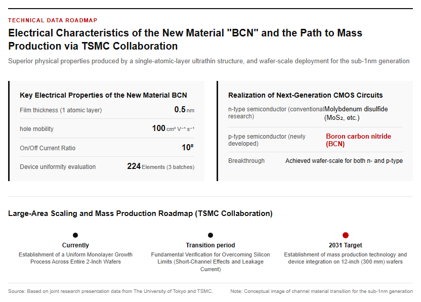
Following the innovative 2D semiconductor development results by the University of Tokyo, Taiwan Semiconductor Manufacturing Company (TSMC), the world’s largest semiconductor foundry, has begun full-scale support and participation in joint research. Based on this achievement, the research team from TSMC and the University of Tokyo aims to establish single-layer film deposition technology and device integration on 12-inch (300 mm) wafers—the global standard production size—by around 2031. TSMC announced the start of mass production for its 2-nanometer (N2) process in December 2025 and is shifting from the conventional FinFET structure to the nanosheet GAA (Gate-All-Around) structure, but has determined that for the sub-1-nanometer ultra-fine generations beyond that, transitioning the channel material itself from silicon to 2D materials is essential. The company invests a massive scale of $20 billion to $30 billion annually in capital expenditures and R&D, and is set to allocate a portion of this into the new material technology originating from the University of Tokyo. The figure below illustrates the generational transition and introduction of new materials in advanced foundries.
The direct incorporation of basic research results from Japanese universities into the next-generation mass-production roadmap of TSMC, which holds global semiconductor hegemony, holds historic significance for industry-academia collaboration.
The Battle for Supremacy at 2nm and Beyond in the Advanced Semiconductor Foundry War
In the global advanced logic semiconductor market, pursuing market leader TSMC, South Korea’s Samsung Electronics, the U.S.’s Intel, and Japan’s Rapidus are engaged in an intense development race. TSMC’s 2nm process “N2” already features hyperscalers and major IC designers such as Apple, NVIDIA, AMD, Qualcomm, Google, and Microsoft among its customers, and is expected to maintain its leadership. However, the design cost for new chips at advanced nodes reaches up to $800 million (approximately 120 billion yen), and manufacturing costs and maintaining yields weigh heavily on all companies. Amidst this, in the “sub-1nm generation,” which will be the primary battlefield following 2nm, how quickly companies can integrate channel material innovations into their own mass-production lines—rather than merely making structural changes—will determine victory or defeat. Behind TSMC’s embrace of 2D material technologies such as the University of Tokyo’s BCN and $\text{MoS}_2$ lies a strategic intent to build a decisive technological barrier to entry against competitors and firmly secure an overwhelming share of the foundry market for the 2030s and beyond.
Spillover Effects on the Stock Market and Related Industries, and Medium-to-Long-Term Outlook
Ripple Effects on Japanese Semiconductor Material and Equipment Manufacturers and Promising Stocks
The industrialization of 2D semiconductors and the realization of wafer-scale mass production will also bring immense business opportunities to Japan’s robust semiconductor materials and manufacturing equipment industries. The deposition of 2D materials requires advanced metalorganic chemical vapor deposition (MOCVD) systems, atomic layer deposition (ALD) systems, and specialized materials such as ultra-high-purity precursor gases. This University of Tokyo research project involves major global semiconductor manufacturing equipment maker Tokyo Electron (TEL) and others as collaborative research institutions, deepening their expertise toward the commercialization of cutting-edge deposition equipment compatible with 2D materials. According to market research, the market size for 2D materials is projected to expand from approximately $350 million (approx. 50 billion yen) in 2025 to $1 billion (approx. 150 billion yen) by 2030, with rapid growth expected at a compound annual growth rate (CAGR) of over 20%. Japanese materials manufacturers and equipment makers—many of which boast top global market shares in various components—will offset the maturation of traditional silicon-focused markets and, combined with surging demand for AI semiconductors, gain a powerful new driver to propel mid-to-long-term earnings growth.
Challenges and Prospects for the Practical Application of Next-Generation Complementary Metal-Oxide-Semiconductor (CMOS) Circuits
The advent of BCN, a new material with a thickness of just a single atom, has sent shockwaves through the semiconductor industry, but several critical technical challenges must be overcome to achieve the ambitious goal of mass production by 2031. First is the further high-precision control of the substitution positions and concentration of carbon atoms, as well as lowering the growth temperature to be compatible with existing manufacturing processes. Second is the establishment of defect-free, large-area transfer technology onto silicon wafers and oxide substrates, along with improving compatibility with back-end-of-line (BEOL) wiring processes. However, research teams centered around the University of Tokyo have successively announced world-leading achievements in the field of two-dimensional materials, such as the p-type doping of BCN, the discovery of a monolayer self-limiting growth mechanism in molybdenum disulfide (MoS₂), and the successful synthesis of 1-nanometer-diameter semiconductor nanotubes. If these elemental technologies come together, ultra-fine transistors at the single-atom level will be commercialized, contributing to greater power efficiency in AI data centers and dramatic performance enhancements in devices like smartphones. There are high expectations that Japan-originated nanomaterial technology will serve as the core driving force to pioneer the global post-silicon era.
Reference Page
- [University of Tokyo Press Release (High-Performance p-Type 2D Semiconductor BCN)] https://www.t.u-tokyo.ac.jp/press/pr2026-10-01-001
- [Paper Published in Nature] https://www.nature.com/articles/s41586-026-11047-9
- [The University of Tokyo Press Release (Next-Generation Semiconductor MoS₂)] https://www.t.u-tokyo.ac.jp/press/pr2026-01-21-001
【#NextGenSemiconductors #UniversityOfTokyo #TSMC #2DMaterials #EconomyBusiness #SemiconductorStocks #CMOS】


コメント