
ABRIC has upgraded its high-voltage semiconductor for ultrasound diagnostic equipment, achieving single-chip integration of the transmission and reception circuits. Behind this development is the growing need to make portable diagnostic devices smaller and more power-efficient, driven by the spread of home healthcare and telemedicine.
- Key Points on Functional Improvements in High-Voltage Semiconductors and Integrated Transceiver ICs
- The History of the Medical Device Business and the Background of the Socionext Business Acquisition
- Circuit Improvements for High-Voltage Analog Switches and High-Precision Transmission Pulsers
- Ultra-compact, Low-power Technologies and Mobile Medical Solutions
- The Expansion of Home Healthcare and Telemedicine and the Value of Portable Ultrasound Diagnostics
- Global Niche Top Strategy and Key Points to Watch Going Forward
Key Points on Functional Improvements in High-Voltage Semiconductors and Integrated Transceiver ICs
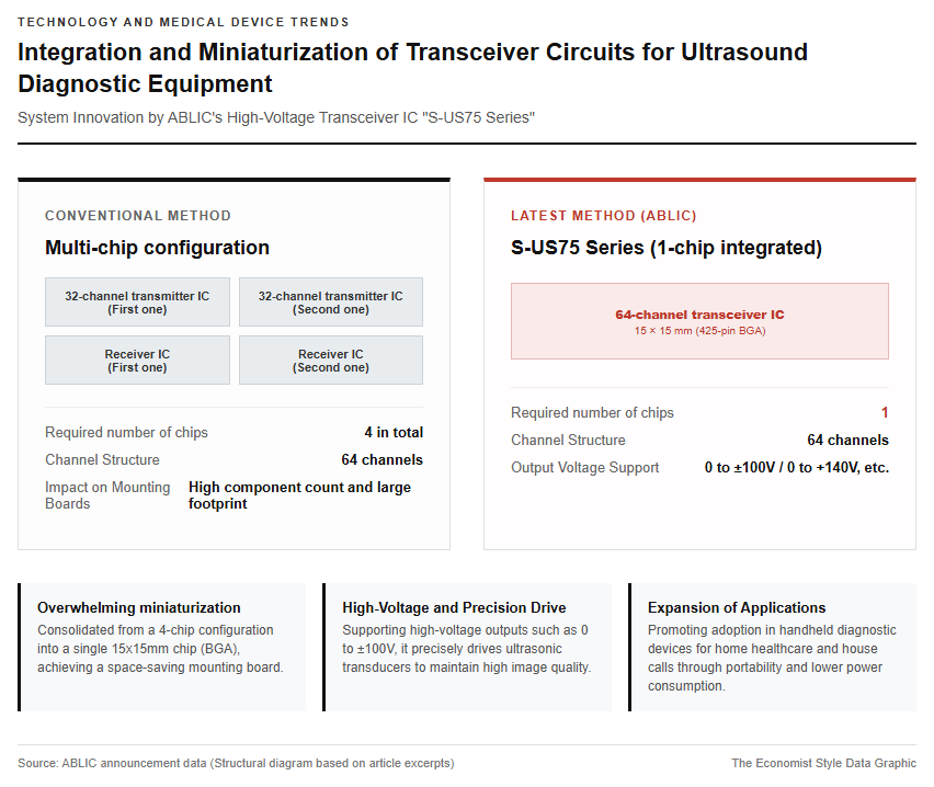
ABLIC, an analog semiconductor manufacturer within the MinebeaMitsumi Group, is advancing functional improvements and expanding solutions for high-voltage semiconductors and front-end ICs used in ultrasonic diagnostic equipment. Specifically, the company has improved the basic performance of its conventionally provided high-voltage transmitter ICs and high-voltage analog switches, while fusing them with the reception technology and LSI design capabilities of the medical-related business acquired from Socionext in December 2024. Through this, high-voltage transceiver ICs such as the “S-US75 series”—which integrates an industry-first 64-channel (64ch) ultrasonic signal transmission circuit and echo signal reception circuit into a single package—have been developed and enhanced.
Traditionally, configuring a 64-ch transceiver circuit required a total of four chips—two 32-ch transmitter ICs and two receiver ICs—but the latest S-US75 series achieves integration into a single chip (a 15×15 mm, 425-pin BGA package). This integration has successfully reduced the number of components on the mounting board, while significantly downsizing the device and lowering power consumption. The output voltage supports high voltages such as 0 to ±100V and 0 to +140V (S-US7503), precisely driving ultrasonic transducers. As a high-voltage compatible semiconductor that achieves both high image quality and portability, it is increasingly being adopted in handheld ultrasonic diagnostic devices used in home healthcare and house-call medical practices. Please refer to the figure below.
The History of the Medical Device Business and the Background of the Socionext Business Acquisition
ABLIC’s semiconductor business for medical devices originated from the acquisition of the related business from Hitachi, Ltd. in 2016. Inheriting the CMOS IC development technology and high-voltage process technology cultivated by Hitachi for over 40 years, the business has secured a high global market share in the fields of transmit pulser ICs and high-voltage analog switches, which are key devices for ultrasonic diagnostic equipment. However, to achieve further miniaturization of diagnostic equipment and higher-definition images, it was essential to optimize the entire system, including not only the transmission side that sends out high-voltage signals, but also the circuit technology that receives and processes extremely weak echo signals from biological tissues with high precision, as well as image generation LSIs.
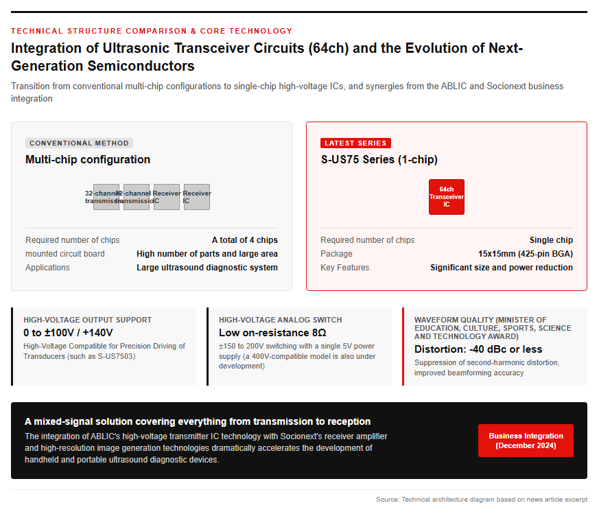
To address these technical challenges, ABLIC acquired Socionext’s medical-related business in December 2024, acquiring advanced receiving amplifier technology, high-resolution image generation technology, and system design capabilities including firmware. Through this business integration, ABLIC’s core strength in high-voltage transmitter IC technology and Socionext’s renowned receiving and image processing technologies perfectly complement one another. The establishment of a mixed-signal solution that consistently covers everything from transmission to reception has dramatically accelerated the development of next-generation wireless diagnostic equipment and portable ultrasound devices.
Key Technologies Supporting the Evolution and Miniaturization of High-Voltage Semiconductors
Circuit Improvements for High-Voltage Analog Switches and High-Precision Transmission Pulsers
Playing a central role in ABLIC’s improvements to high-voltage-compatible semiconductors is the advanced circuit design technology for high-voltage analog switches and ultrasound transmission digital pulsars. The company’s high-voltage analog switches support high-speed switching of high-voltage signals ranging from ±150V to 200V, despite operating on a single 5V control power supply. They feature low on-resistance (such as 8Ω) that is independent of signal voltage fluctuations and low charge injection characteristics, and development of 400V-compatible products is also underway for next-generation equipment.
In the ultrasonic transmission pulser circuit, we adopted a perfectly matched design for the P-channel and N-channel MOSFETs of the high-voltage output driver circuit, along with active ground clamping technology. This suppresses distortion in the pulse waveform and achieves an exceptional positive-negative symmetrical output waveform with second-harmonic distortion kept below -40dBc. The patent for this waveform quality improvement technology received high acclaim, winning the Minister of Education, Culture, Sports, Science and Technology Award at the 2024 Kanto Region Invention Awards. Furthermore, the reduction in jitter and channel-to-channel propagation delay error through the clock synchronization function dramatically improves beamforming accuracy, enabling clear imaging of deep tissues. Please refer to the figure below.
Ultra-compact, Low-power Technologies and Mobile Medical Solutions
Since developing the world’s first mass-produced CMOS IC for quartz watches in 1968, ABLIC has pursued ultra-miniaturization and low-power consumption technologies for over half a century. This accumulation of analog semiconductor technology has also deeply contributed to the evolution of medical ICs. For its “viewphii” mobile medical device solution series, the company offers a two-chip set consisting of a pulser LSI compatible with 64-element ultrasonic transducers and an ultrasound image generation LSI.
In addition, by combining an 8-channel 12-bit 50MSPS high-speed ADC for received signal processing (S-US85A1) and a 32-channel high-voltage analog switch (S-UM6522E), direct mounting on the probe’s internal board has been made possible. The ADC circuit features a register-switchable low-power operation mode (reducing power consumption from 138 mW/ch in normal operation to 78 mW/ch in low-power mode), enabling long hours of continuous operation in battery-powered wireless ultrasound diagnostic equipment. The company also offers a printed wiring board for evaluation (viewphii64-PCB), four types of prototype probes tailored to specific applications, and evaluation boards, strongly supporting the efficiency of prototyping and evaluation for medical device manufacturers.
The Social Significance of the Medical Field and MinebeaMitsumi’s Growth Strategy
The Expansion of Home Healthcare and Telemedicine and the Value of Portable Ultrasound Diagnostics
The integration and performance improvement of high-voltage compatible semiconductors are making a major contribution to transforming diagnostic styles in medical settings. Conventionally, large stationary ultrasound diagnostic equipment was limited to hospital examination rooms and similar locations, but thanks to circuit miniaturization and lower power consumption, the adoption of pocket-sized handheld devices is accelerating. This has enabled physicians during house calls—such as in home-based medical care and visiting nursing accompanying an aging population, emergency response sites, and telemedicine in depopulated areas—to visually inspect internal tissues and blood flow on the spot.
Furthermore, the applications of ultrasound diagnosis continue to expand, including checking for muscle and tendon injuries in orthopedic surgery, providing immediate diagnosis in sports medicine, and enabling online health checkups where pregnant women use testing kits at home to collect and transmit abdominal data to medical institutions. Through the integration of ultrasound image data, smart devices, and AI-powered diagnostic support technology, it is expected to solve social issues such as the early detection of diseases, the reduction of medical expenses, and the extension of healthy life expectancy. Continuous technological innovation in high-voltage compatible semiconductors serves as a vital technical foundation supporting the forefront of sustainable medical DX (digital transformation).
Global Niche Top Strategy and Key Points to Watch Going Forward
Within the MinebeaMitsumi Group, the analog semiconductor business operated by ABLIC is positioned as the second spear of the “Eight Spears”—the group’s core businesses—and is driving the group’s growth. The company avoids highly competitive general-purpose mass-production fields and promotes the “niche top strategy (the strategy of becoming the biggest fish in the pond)” to secure an overwhelming share in technologically challenging niche fields. It aims to achieve overall sales of 200 billion yen and an operating profit margin of 30% for the semiconductor division by the fiscal year ending March 2029, with ICs for medical devices being one of its priority areas.
Moving forward, leveraging its strengths as an IDM (Integrated Device Manufacturer) that handles everything from circuit design to in-house fab manufacturing, the company plans to further strengthen the rollout of “analog-digital integrated” products that incorporate large-scale digital logic into analog circuits. In addition, high-voltage control technology in the ±150V to 400V class and high-precision pulse generation technology, both honed in the medical field, are being horizontally deployed into industrial sensing applications such as non-destructive testing equipment for infrastructure and sonar detection systems for water quality and environmental monitoring. With the integration of transmission and reception technologies, future developments will be closely watched to see if ABLIC can achieve further growth in the global market.
Reference Page
- [Optimal Solution for Handheld/Compact Ultrasound Equipment – ABLIC Inc.] https://www.ablic.com/jp/semicon/healthcare/solution-for-handheld-ultrasound-equipment/
- [ICs for Medical Devices – ABLIC Inc.] https://www.ablic.com/jp/semicon/healthcare/
- [Ultrasonic Transmission Digital Pulser – ABLIC Inc.] https://www.ablic.com/jp/semicon/healthcare/digital-pulser/
- 【ABLIC Strengthens Semiconductor Portfolio for Ultrasound Diagnostic Equipment through Acquisition of Socionext’s Medical-Related Business – ABLIC Inc.】https://www.ablic.com/jp/semicon/news/2025/04/08/healthcare_content/
[#UltrasoundDiagnosticEquipment #HighVoltageSemiconductors #ABLIC #MedicalDevices #AnalogICs #HandheldMedical #MinebeaMitsumi]


コメント